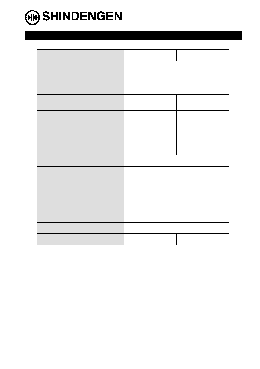
CME3.3V4 A /5V 7A
5
3.3
Output voltage
( V )
- 48
Input voltage
( V )
- 36 ~ - 60
Input voltage range
( V )
- 53
Conduction noise
(dBm)
+ 5%
- 5%
+ 5%
- 5%
Output voltage range
7
4
Output Current
( A )
0 ~ 7
0 ~ 4
Output current range
( A )
10.5
6
Over current protection ( A )
6
4.2
Over voltage protection ( V )
100
Output ripple noise ( mVp-p )
85 %
Efficiency
Ta = 0 ~70
∞
C
Operating temparature
61.0
◊
97.0
◊
8.5
Mechanical dimension ( mm )
AC 500, DC 707 (applied for 1minute)
Isolated voltage
( V )
Parallel operation
Forced air cooling (1.5m /sec)
Cooling method
4.5
2.5
Low voltage protection ( V )
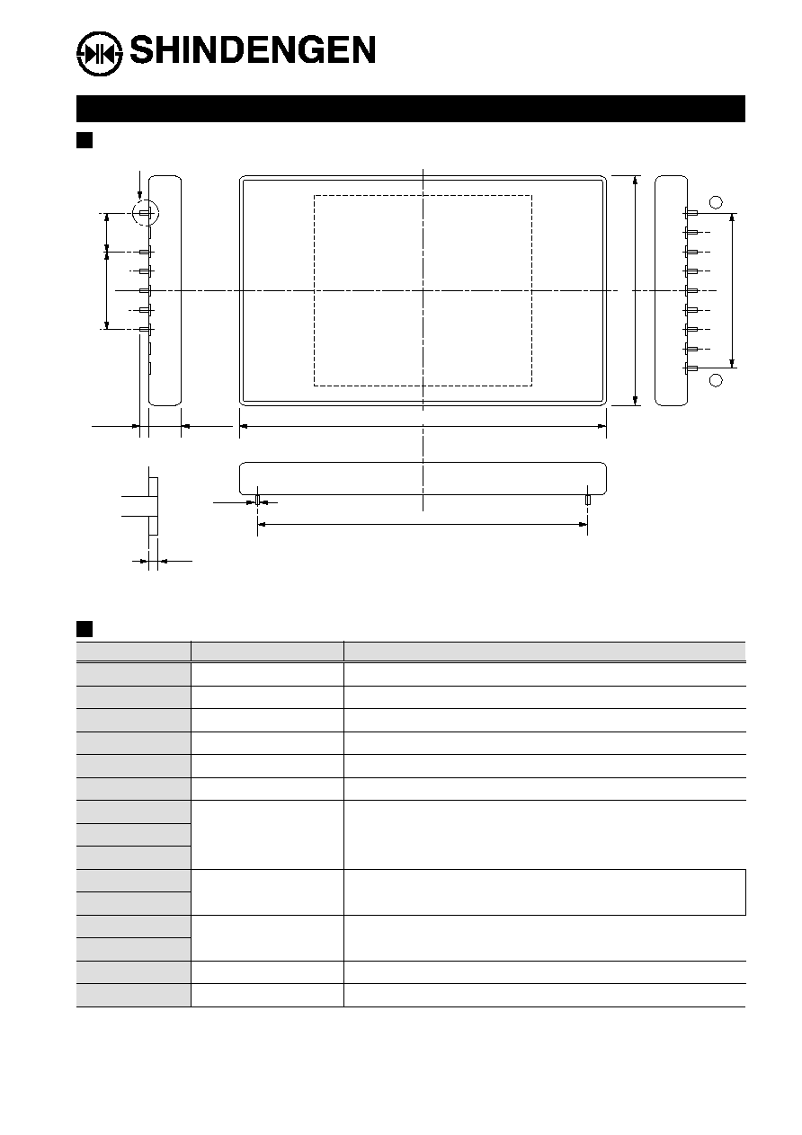
CME3.3V4 A /5V 7A
Function
Symbol
Pin No.
Output power down signal pin
PS
1
Local off control signal pin
LO
2
Alarm pin
P
3
SAB pin
SAB
4
Input voltage pin
-IN
5
Input ground pin
+IN
6
Output ground pin
0 V
7
8
9
Output voltage pin
+ 3.3 V
10
11
Output voltage pin
+ 5 V
12
13
Not connected*
T T1
14
Not connected*
T T2
15
*NC may be used for testing by the manufacturer and shall not be connected by the customer.
Outline diagram
Pin arrangement
86.36
±
0.5
0.8
±
0.2
1.0
A
15
7
10.16
4
◊
5.08=20.32
2.5MIN
8.5MAX
96.0
±
1.0
60.0
±
1.0
8
◊
5.08=
40.64
* Dimentions are in millimeters.
Enlargement picture of A
5/1