
400V 15A
Copyright & Copy;2002 Shindengen Electric Mfg.Co.,Ltd.
OUTLINE DIMENSIONS
(Unit : mm)
RATINGS
SHINDENGEN
Case : D15VD
Dual Modules
D15VD40
General Purpose Rectifiers
Absolute Maximum Ratings
Item
Symbol
Conditions
Ratings
Unit
Storage Temperature
Tstg
-40`150
Operating Junction Temperature
Tj
150
Maximum Reverse Voltage
V
RM
400
V
Average Rectified Forward Current
I
O
50Hz sine wave Voltage doubler rectification, Tc=94
15
A
50Hz sine wave at:Brigde resistance load, Tc=94
18
Peak Surge Forward Current
I
FSM
Non-repetitive 50Hz sine wave Tj=25
400
A
Dielectric Strength
Vdis
Terminals to case, AC 1 minute
2
kV
Mounting Torque
TOR
i j Shows recommended value
2(1)
NEm
Electrical Characteristics (If not specified Tc=25)
Item
Symbol
Conditions
Ratings
Unit
Forward Voltage
V
F
I
F
=15A, Rating of per diode
Max.1.05
V
Reverse Current
I
R
V
R
=V
RM
,
Rating of per diode
Max.10
A
Thermal Resistance
∆jc
junction to case
Max.3.5
/W
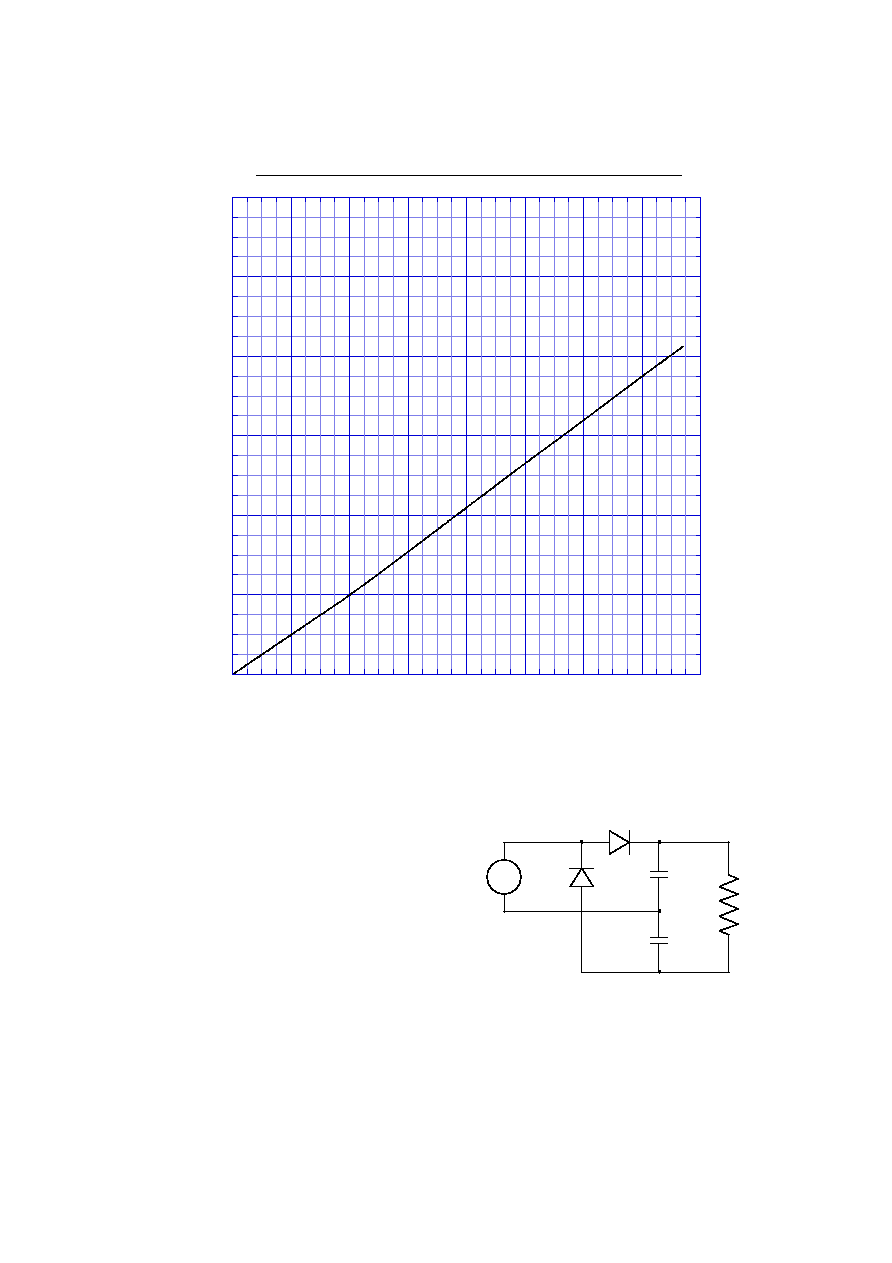
Doubler type

0
5
10
15
20
25
30
0
5
10
15
20
25
D15VD40
Forward Power Dissipation
Tj = 150
∞
C
Sine wave
R-load
Single phase rectification
~
I
O
Average Rectified Forward Current I
O
[A]
Forward Power Dissipation P
F
[W]
0
4
8
12
16
20
24
0
2
4
6
8
10
12
14
16
D15VD40
Forward Power Dissipation
Tj = 150
∞
C
Sine wave
Voltage doubler rectification
~
Average Rectified Forward Current I
O
[A]
Forward Power Dissipation P
F
[W]

0
I
O
0
2
4
6
8
10
12
14
16
0
2
4
6
8
10
12
14
D15VD40
Forward Power Dissipation
Tj = 150
∞
C
Sine wave
R-load
per diode
Average Rectified Forward Current I
O
[A]
Forward Power Dissipation P
F
[W]
