
D1F60A
600V 1.2A
Copyright & Copy;2000 Shindengen Electric Mfg.Co.Ltd
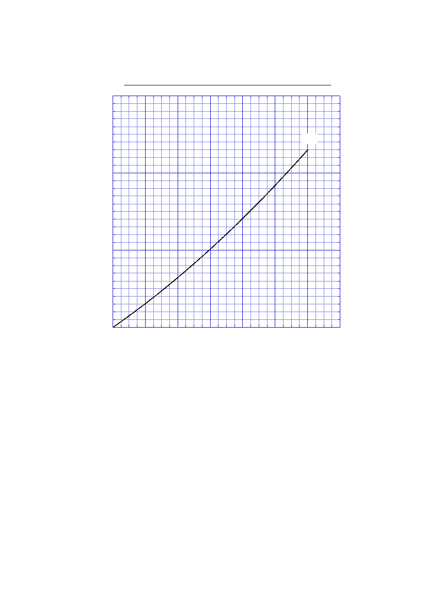
OUTLINE DIMENSIONS
RATINGS
SHINDENGEN
Case : 1F
Unit : mm
Single
General Purpose Rectifiers
Absolute Maximum Ratings (If not specified Tl=25)
Item
Symbol
Conditions
Ratings
Unit
Storage Temperature
Tstg
-55150
Operating Junction Temperature
Tj
150
Maximum Reverse Voltage
V
RM
600
V
Average Rectified Forward Current
I
O
50Hz sine wave, R-load, Ta=25 On alumina substrate
1.2
A
50Hz sine wave, R-load, Ta=25 On glass-epoxy substrate
0.88
Peak Surge Forward Current
I
FSM
50Hz sine wave, Non-repetitive 1 cycle peak value, Tj=25
45
A
Current squared time
I
2
t
1mst10
8
A
2
s
Electrical Characteristics (If not specified Tl=25)
Item
Symbol
Conditions
Ratings
Unit
Forward Voltage
V
F
I
F
=1.2A, Pulse measurement
Max.0.97
V
Reverse Current
I
R
V
R
=V
RM
,
Pulse measurement
Max.10
A
jl
junction to lead
Max.23
Thermal Resistance
ja
junction to ambient On alumina substrate
Max.108
/W
junction to ambient On glass-epoxy substrate
Max.157
0
0.5
1
1.5
0
0.2
0.4
0.6
0.8
1
1.2
1.4
D1F60A
Forward Power Dissipation
SIN
Average Rectified Forward Current I
O
[A]
Forward Power Dissipation P
F
[W]
Tj = 150
∞
C
Sine wave

0
t
p
I
O
T
D=t
p
/T
0
20
40
60
80
100
120
140
160
0
0.5
1
1.5
2
D1F60A
Derating Curve
V
R
= V
RM
SIN
0
V
R
Alumina substrate
Soldering land 2mm
Conductor layer 20
µ
m
Substrate thickness 0.64mm
Ambient Temperature Ta [
∞
C]
Average Rectified Forward Current I
O
[A]

