D4SBL40
D4SBL40
400V 4A
400V 4A
Copyright & Copy;2000 Shindengen Electric Mfg.Co.Ltd
Copyright & Copy;2000 Shindengen Electric Mfg.Co.Ltd
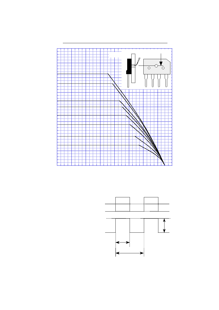
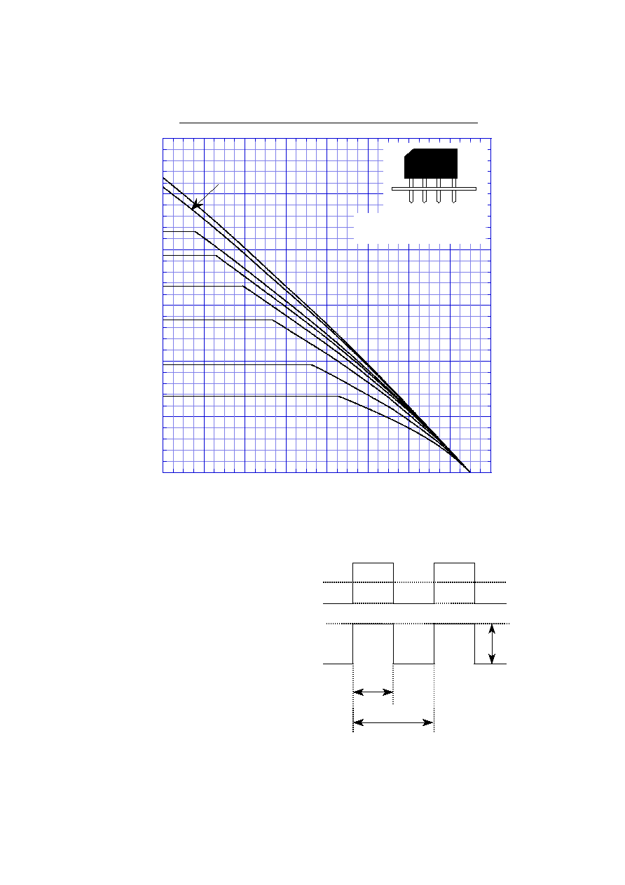
OUTLINE DIMENSIONS
OUTLINE DIMENSIONS
(Unit : mm)
(Unit : mm)
RATINGS
RATINGS
SHINDENGEN
SHINDENGEN
Switching power supply
Switching power supply
Home (Electrical) Appliances
Home (Electrical) Appliances
Office Equipment, Telecommunication,
Office Equipment, Telecommunication,
Factory Automation
Factory Automation
APPLICATION
APPLICATION
Low noise
Low noise
SIL Package
SIL Package
High IFSM
High IFSM
FEATURES
FEATURES
Case : 3S
Case : 3S
Super Fast Recovery Rectifiers
Super Fast Recovery Rectifiers
Super Fast Bridges
Super Fast Bridges
Absolute Maximum Ratings (If not specified Tc=25)
Item
Symbol
Conditions
Ratings
Unit
Storage Temperature
Tstg
-55150
Operating Junction Temperature
Tj
150
Maximum Reverse Voltage
V
RM
400
V
Average Rectified Forward Current
I
O
50Hz sine wave, R-load With heatsink Tc=91
4
A
50Hz sine wave, R-load Without heatsink Ta=25
1.95
Peak Surge Forward Current
I
FSM
50Hz sine wave, Non-repetitive 1cycle peak value, Tj=25
50
A
Dielectric Strength
Vdis
Terminals to case, AC 1 minute
2
kV
Mounting Torque
TOR
Recommended torque
0.5Nm
0.8
Nm
Electrical Characteristics (If not specified Tl=25)
Item
Symbol
Conditions
Ratings
Unit
Forward Voltage
V
F
I
F
=2.5A, Pulse measurement, Rating of per diode
Max.1.3
V
Reverse Current
I
R
V
R
=V
RM
,
Pulse measurement, Rating of per diode
Max.10
A
Reverse Recovery Time
trr
I
F
= 0.5A, I
R
= 1A
Max.50
ns
jc
junction to case With heatsink
Max.5.5
Thermal Resistance
jl
junction to lead Without heatsink
Max.6
/W
ja
junction to ambient Without heatsink
Max.30

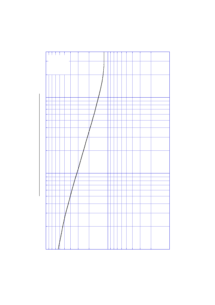
Peak Surge Forward Capability
0
10
20
30
40
50
60
70
80
1
10
100
D4SBL40
2
5
20
50
I
FSM
10ms 10ms
1 cycle
Number of Cycles [cycles]
Peak Surge Forward Current I
FSM
[A]
non-repetitive,
sine wave,
Tj=25
∞
C before
surge current is applied