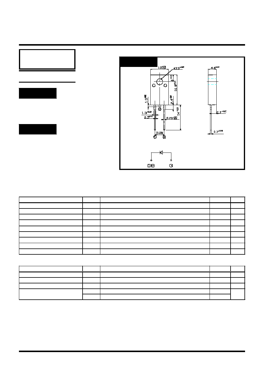
D5S4M
40V 5A
Copyright & Copy;2000 Shindengen Electric Mfg.Co.Ltd
OUTLINE DIMENSIONS
Unit : mm
SHINDENGEN
Case : ITO-220
RATINGS
Tj150
P
RRSM
avalanche guaranteed
Fully Isolated Molding
FEATURES
APPLICATION
Switching power supply
DC/DC converter
Home Appliances, Office Equipment
Telecommunication
Absolute Maximum Ratings (If not specified T=25)
Item
Symbol
Conditions
Ratings
Unit
Storage Temperature
Tstg
-40150
Operating Junction Temperature
Tj
150
Maximum Reverse Voltage
V
RM
40
V
Repetitive Peak Surge Reverse Voltage
V
RRSM
Pulse width 0.5ms, duty1/40
45
V
Average Rectified Forward Current
I
O
50Hz sine wave,R-load, Tc=131
5
A
Peak Surge Forward Current
I
FSM
50Hz sine wave,Non-repetitive 1 cycle peak value, Tj=125
100
A
Repetitive Peak Surge Reverse Power
P
RRSM
Pulse width 10s, Tj=25
330
W
Dielectric Strength
Vdis
Terminals to case, AC 1 minute
1.5
kV
Mounting Torque
TOR
(Recommended torque
0.3Nm)
0.5
Nm
Electrical Characteristics (If not specified T=25)
Item
Symbol
Conditions
Ratings
Unit
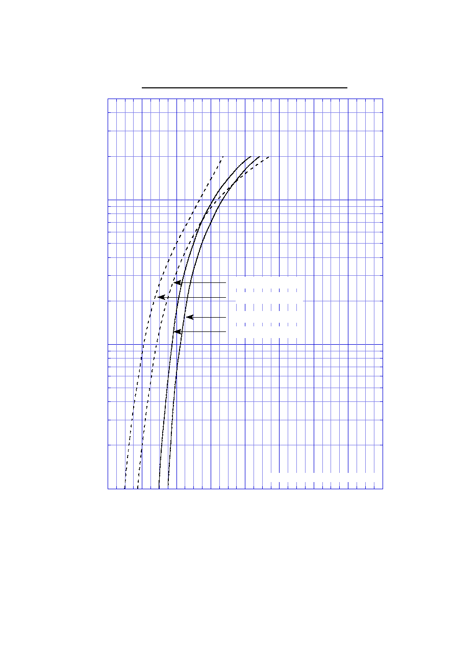
Forward Voltage
V
F
I
F
=5A, Pulse measurement
Max.0.55
V
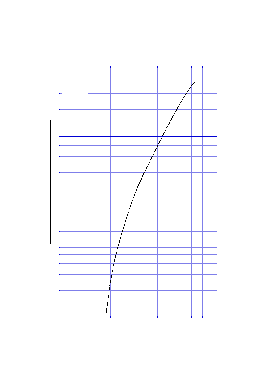
Reverse Current
I
R
V
R
=V
RM
, Pulse measurement
Max. 3.5
mA
Junction Capacitance
Cj
f=1MHz, V
R
=10V
Typ.180
pF
Thermal Resistance
jc
junction to case
Max.4.5
/W
cf
case to heatsink
Max.1.5
Single
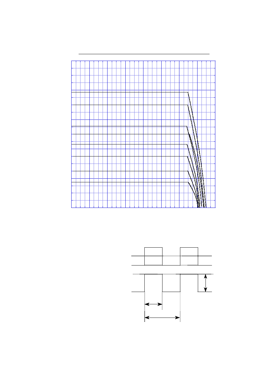
Schottky Rectifiers (SBD)
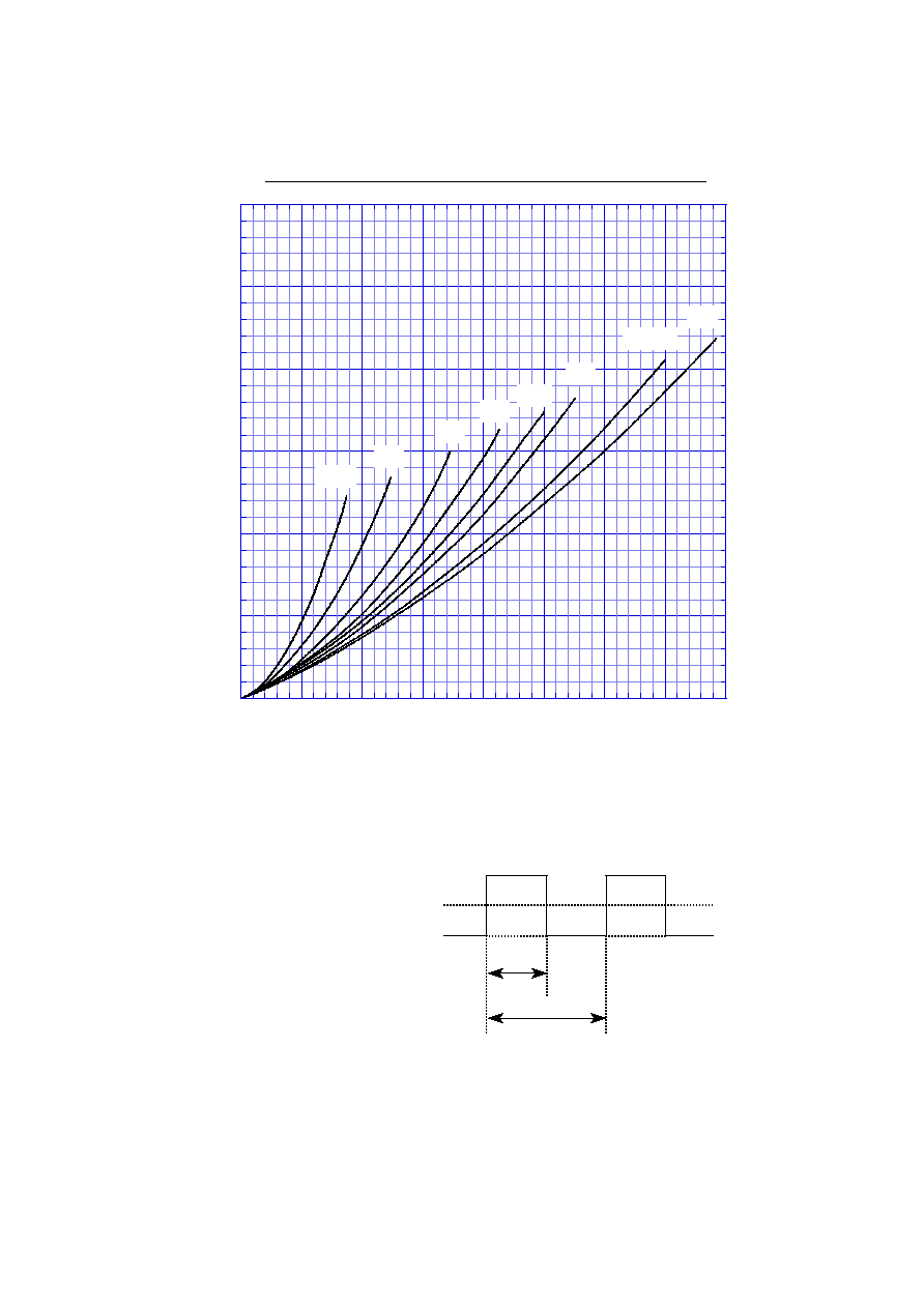
0
t
p
I
O
T
D=t
p
/T
0
1
2
3
4
5
6
0
1
2
3
4
5
6
7
8
D5S4M
0.3
Forward Power Dissipation
Tj = 150
∞
C
SIN
0.2
0.1
D=0.8
DC
0.5
0.05
Average Rectified Forward Current I
O
[A]
Forward Power Dissipation P
F
[W]
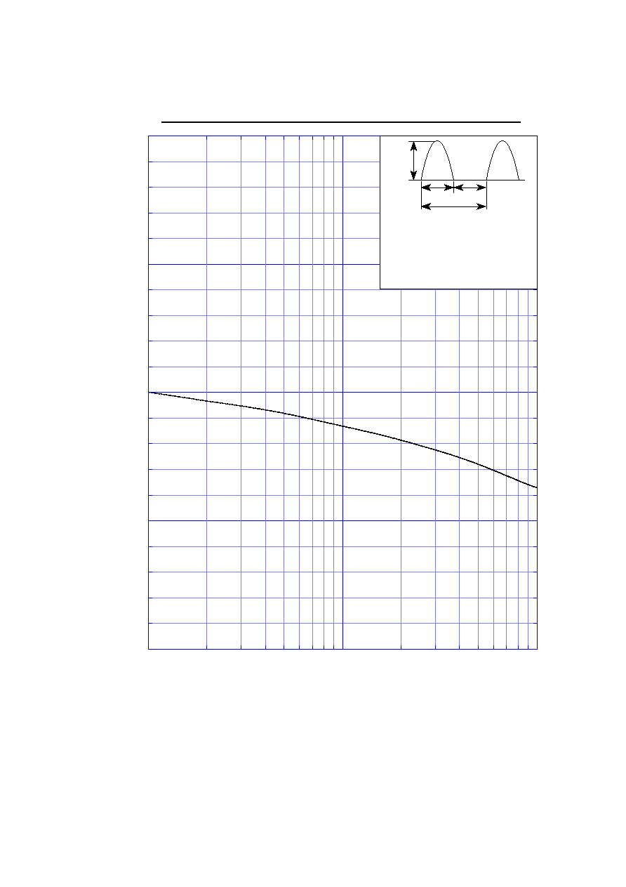
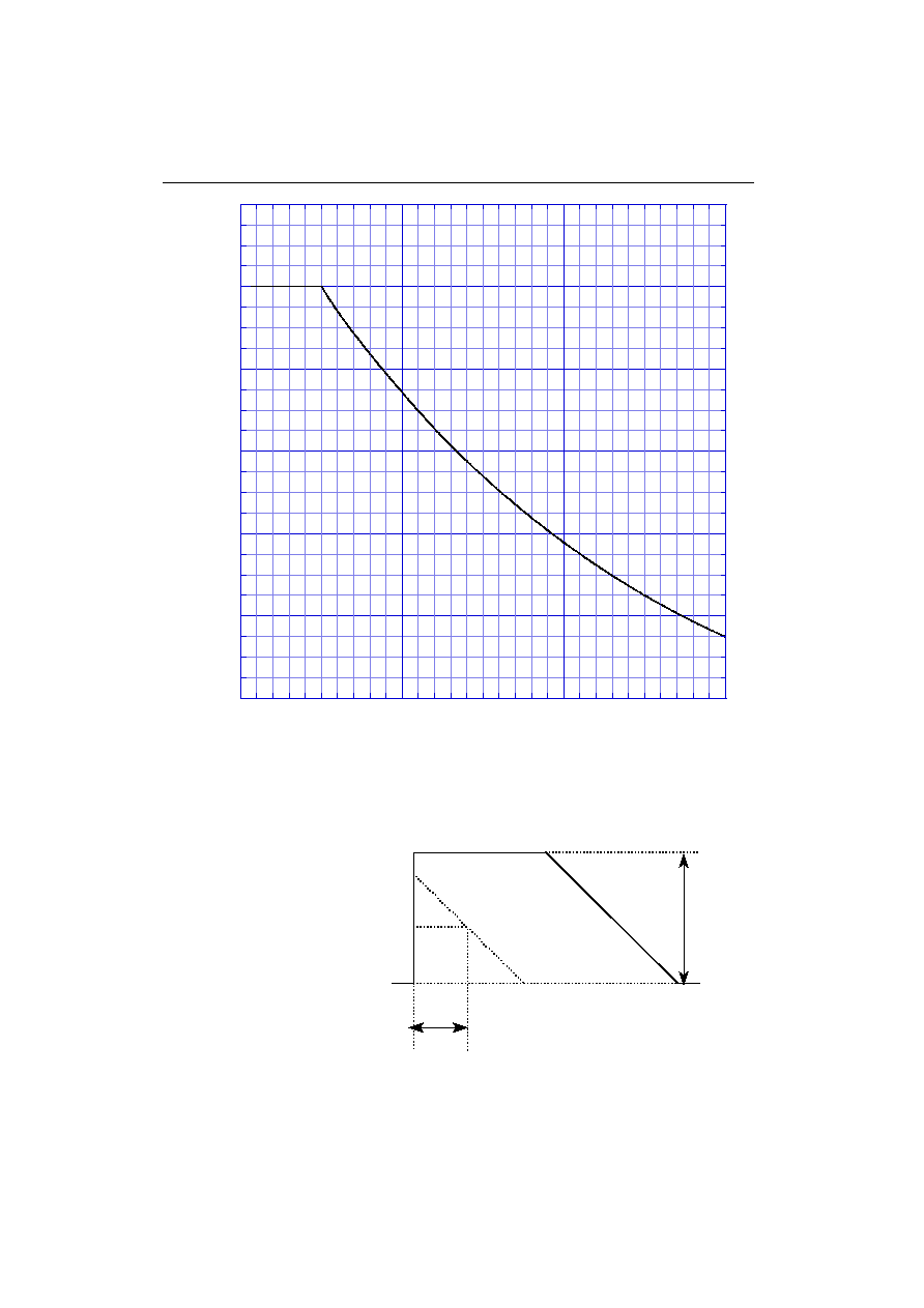
Peak Surge Forward Capability
0
50
100
150
200
1
10
100
D5S4M
2
5
20
50
I
FSM
10ms 10ms
1 cycle
Number of Cycles [cycles]
Peak Surge Forward Current I
FSM
[A]
non-repetitive,
sine wave,
Tj=125
∞
C before
surge current is applied