
DF10LC30
300V 10A
Copyright & Copy;2001 Shindengen Electric Mfg.Co.Ltd
OUTLINE DIMENSIONS
Unit : mm
RATINGS
SHINDENGEN
Case : STO-220
Dual
Super Fast Recovery Rectifiers
Absolute Maximum Ratings (Unless otherwise specified, Tc=25)
Item
Symbol
Conditions
Ratings
Unit
Storage Temperature
Tstg
-55`150
Operating Junction Temperature
Tj
150
Maximum Reverse Voltage
V
RM
300
V
Average Rectified Forward Current
I
O
50Hz sine wave, R-load, Rating for each diode Io/2, Tc=124
10
A
Peak Surge Forward Current
I
FSM
50Hz sine wave, Non-repetitive 1 cycle peak value, Tj=25
80
A
Electrical Characteristics (Unless otherwise specified, Tc=25)
Item
Symbol
Conditions
Ratings
Unit
Forward Voltage
V
F
I
F
=5A, Pulse measurement, Rating of per diode
Max 1.3
V
Reverse Current
I
R
V
R
=V
RM
, Pulse measurement, Rating of per diode
Max 25
A
Reverse Recovery Time
trr
I
F
=0.5A,@ I
R
=1A,@ Rating of per diode
Max 30
ns
Junction Capacitance
Cj
f=1MHz, V
R
=10V, Rating of per diode
TYP 50
pF
Thermal Resistance
∆jc
junction to case
Max 2.0 /W
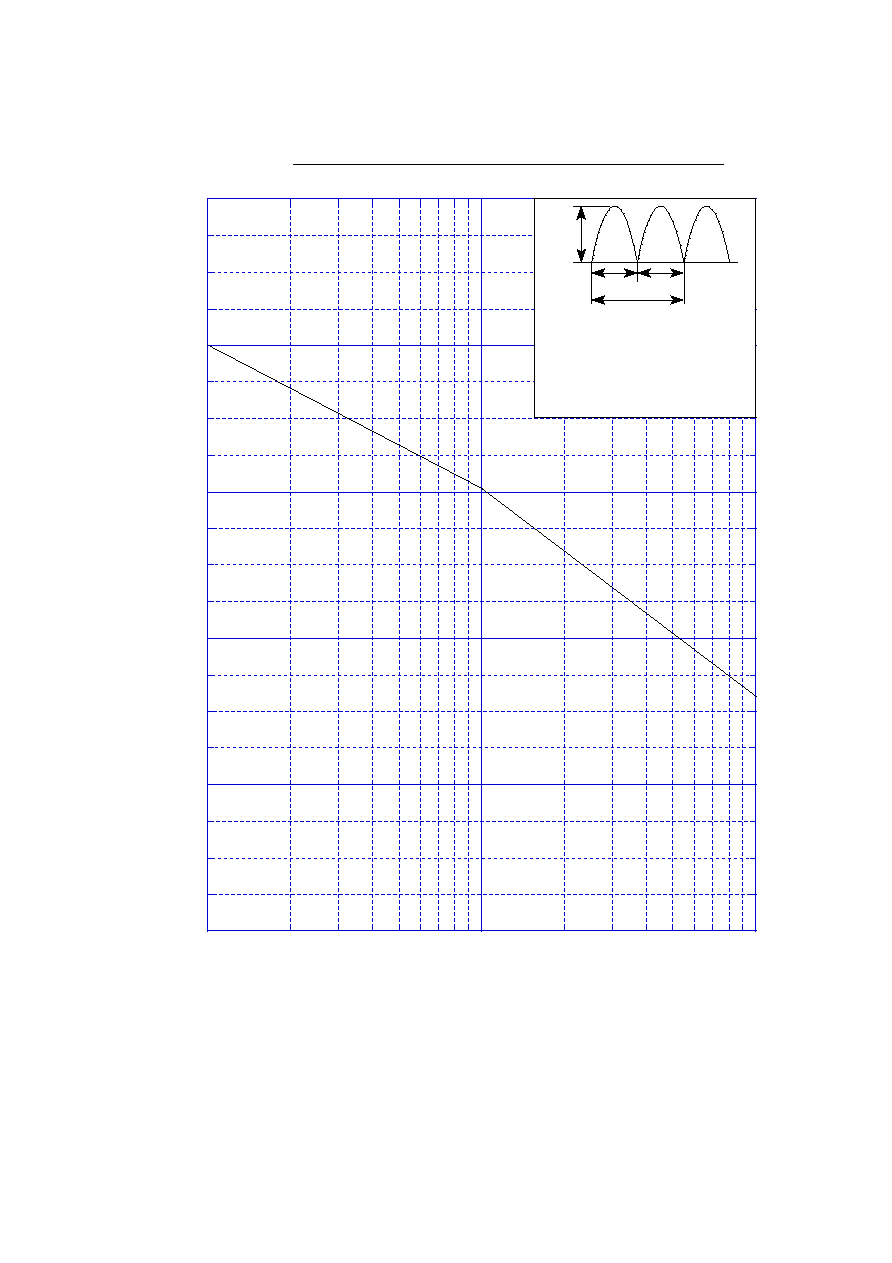
0
20
40
60
80
100
1
10
100
DF10LC30
Peak Surge Forward Capability
Number of Cycles
[cycle]
I
FS
M
[A]
P
eak
S
u
r
g
e F
o
r
w
ar
d
C
u
r
r
e
n
t
I
FS
M
10ms 10ms
1 cycle
non-repetitive,
sine wave,
Tj=25∞C before
surge current is applied


