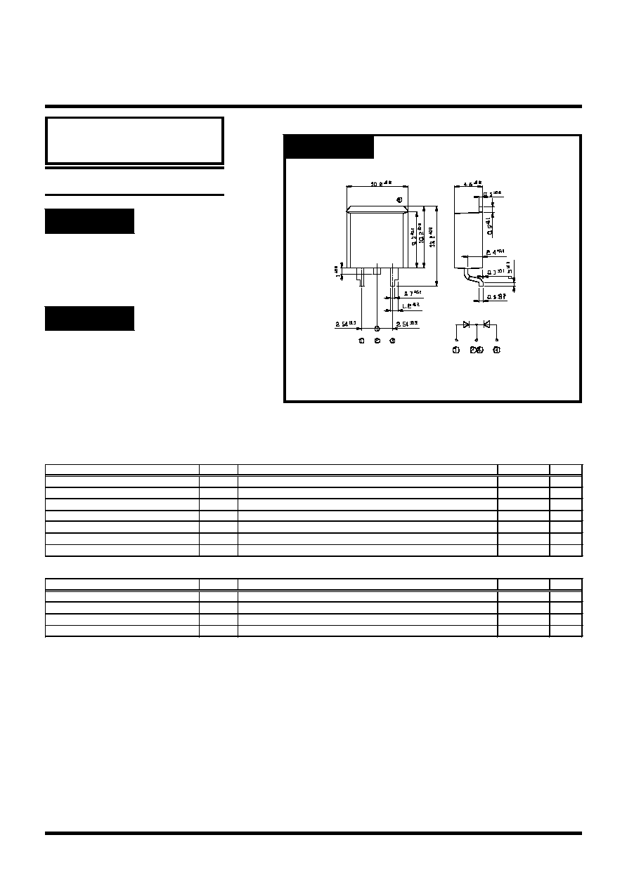
DF20SC9M
90V 20A
Copyright & Copy;2000 Shindengen Electric Mfg.Co.Ltd
SHINDENGEN
OUTLINE DIMENSIONS
Unit : mm
RATINGS
Case : STO-220
SMT
Tj150
P
RRSM
avalanche guaranteed
High current capacity with Small Package
Switching power supply
DC/DC converter
Home Appliances, Office Equipment
Telecommunication
FEATURES
APPLICATION
Schottky Rectifiers (SBD)
Dual
Absolute Maximum Ratings (If not specified Tc=25)
Item
Symbol
Conditions
Ratings
Unit
Storage Temperature
Tstg
-40150
Operating Junction Temperature
Tj
150
Maximum Reverse Voltage
V
RM
90
V
Repetitive Peak Surge Reverse Voltage
V
RRSM
Pulse width 0.5ms, duty 1/40
100
V
Average Rectified Forward Current
I
O
50Hz sine wave, R-load, Rating for each diode Io/2, Tc=111
20
A
Peak Surge Forward Current
I
FSM
50Hz sine wave, Non-repetitive 1 cycle peak value, Tj=25
200
A
Repetitive Peak Surge Reverse Power
P
RRSM
Pulse width 10s, Rating of per diode, Tj=25
660
W
Electrical Characteristics (If not specified Tc=25)
Item
Symbol
Conditions
Ratings
Unit
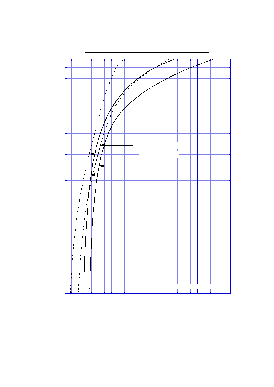
Forward Voltage
V
F
I
F
=10A, Pulse measurement, Rating of per diode
Max.0.75
V
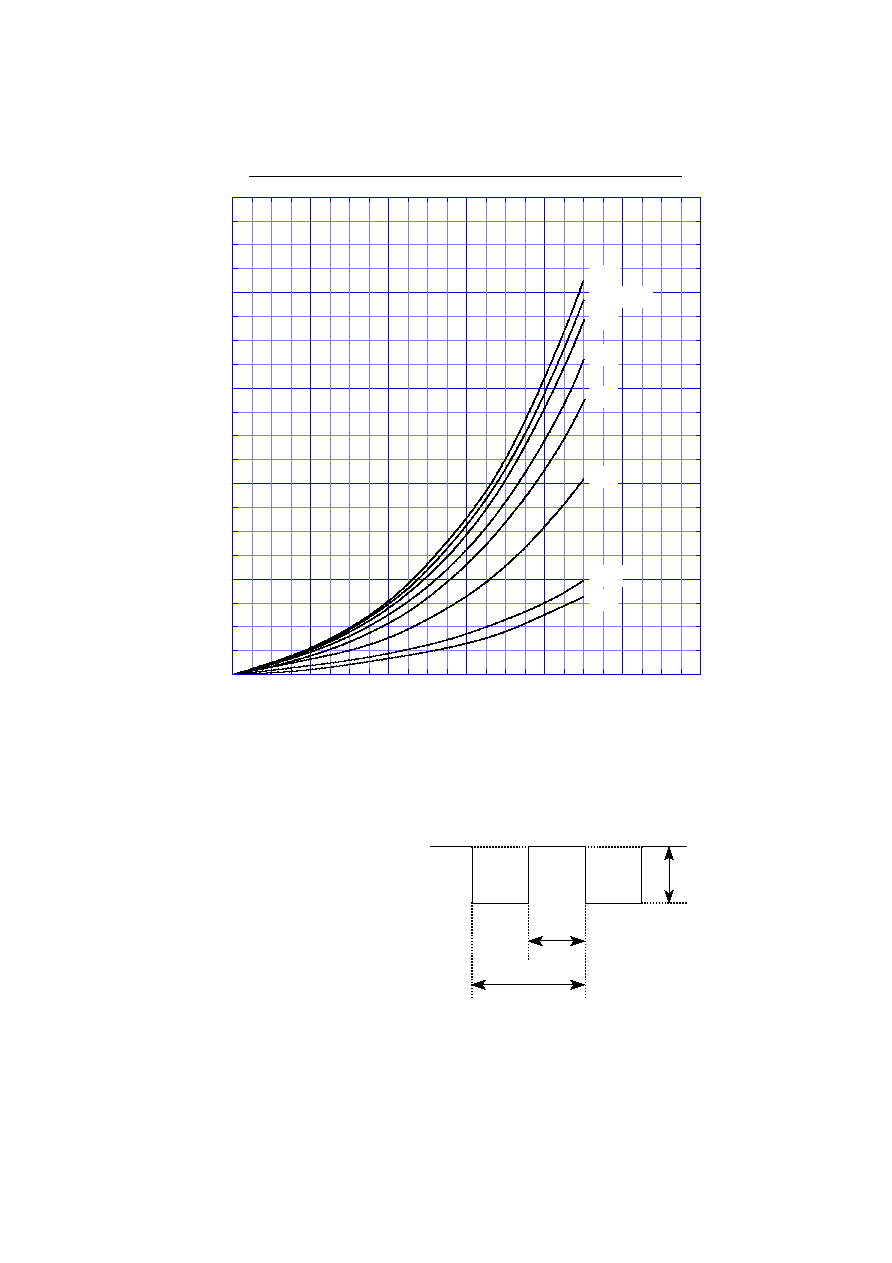
Reverse Current
I
R
V
R
=V
RM
, Pulse measurement, Rating of per diode
Max.10
mA
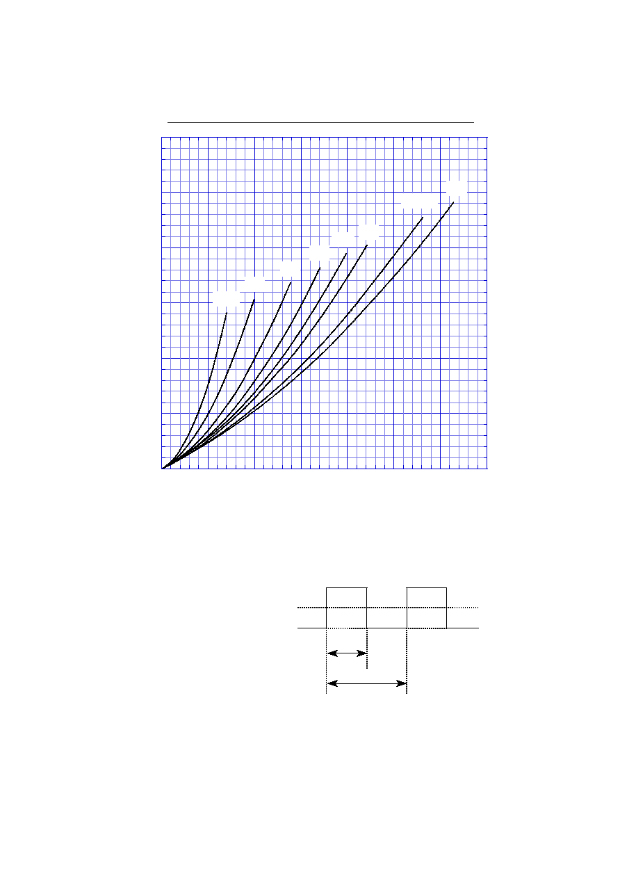
Junction Capacitance
Cj
f=1MHz, V
R
=10V, Rating of per diode
Typ.370
pF
Thermal Resistance
jc
junction to case
Max.1.6 /W
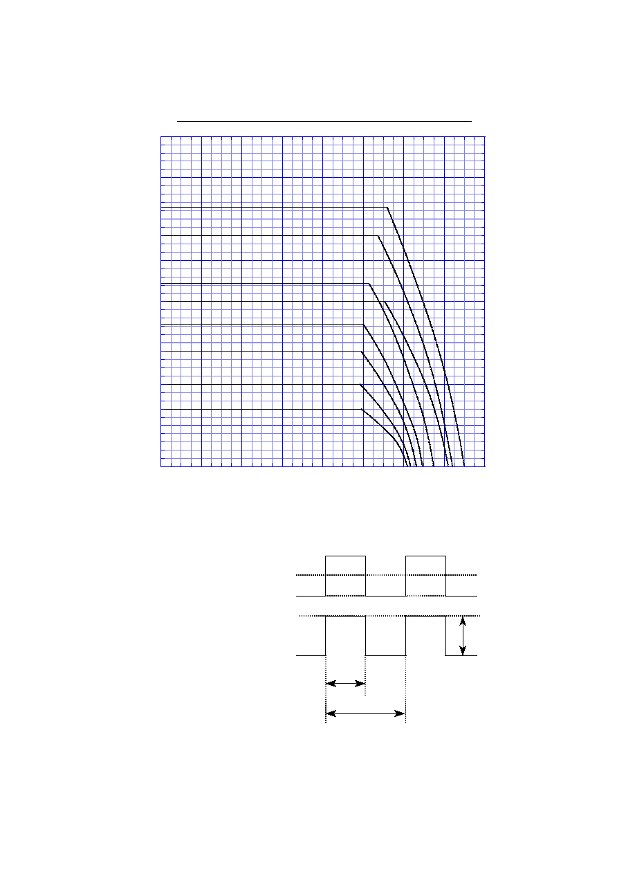
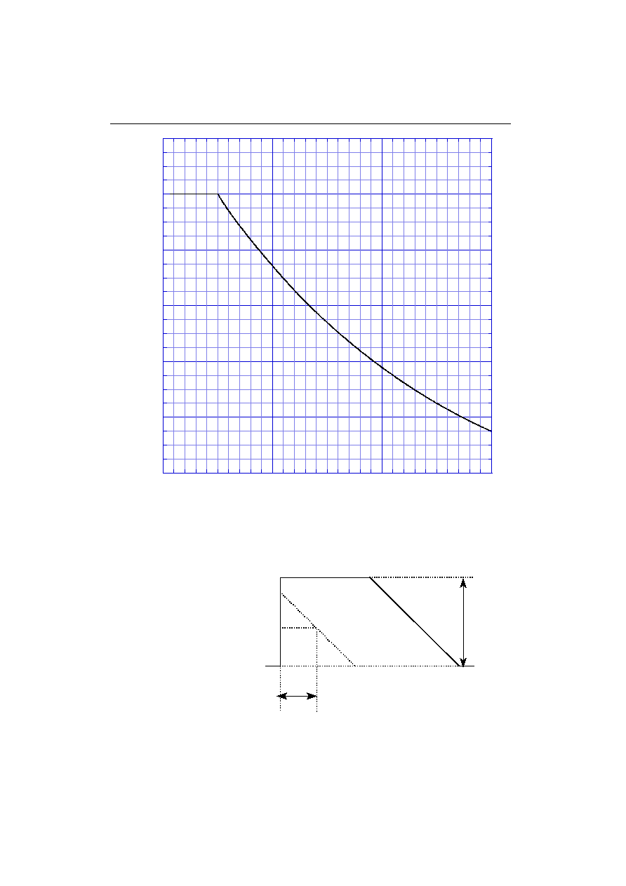
Peak Surge Forward Capability
0
50
100
150
200
250
300
1
10
100
DF20SC9M
2
5
20
50
I
FSM
10ms 10ms
1 cycle
Number of Cycles [cycles]
Peak Surge Forward Current I
FSM
[A]
non-repetitive,
sine wave,
Tj=25
°
C before
surge current is applied