DF40PC3
30V 40A
Copyright & Copy;2000 Shindengen Electric Mfg.Co.Ltd
SHINDENGEN
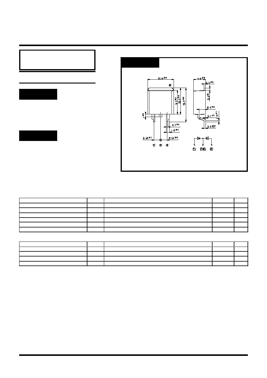
OUTLINE DIMENSIONS
Unit : mm
RATINGS
Case : STO-220
SMT
Super low V
F
=0.4V
High current capacity with Small Package
Reversed Battery Connection Protection
DC OR output
DC/DC converter
Mobile telephone, personal computer
FEATURES
APPLICATION
Dual
Schottky Rectifiers (SBD)
Absolute Maximum Ratings (If not specified Tc=25)
Item
Symbol
Conditions
Ratings
Unit
Storage Temperature
Tstg
-55125
Operating Junction Temperature
Tj
125
Maximum Reverse Voltage
V
RM
30
V
Repetitive Peak Surge Reverse Voltage
V
RRSM
Pulse width 0.5ms, duty 1/40
35
V
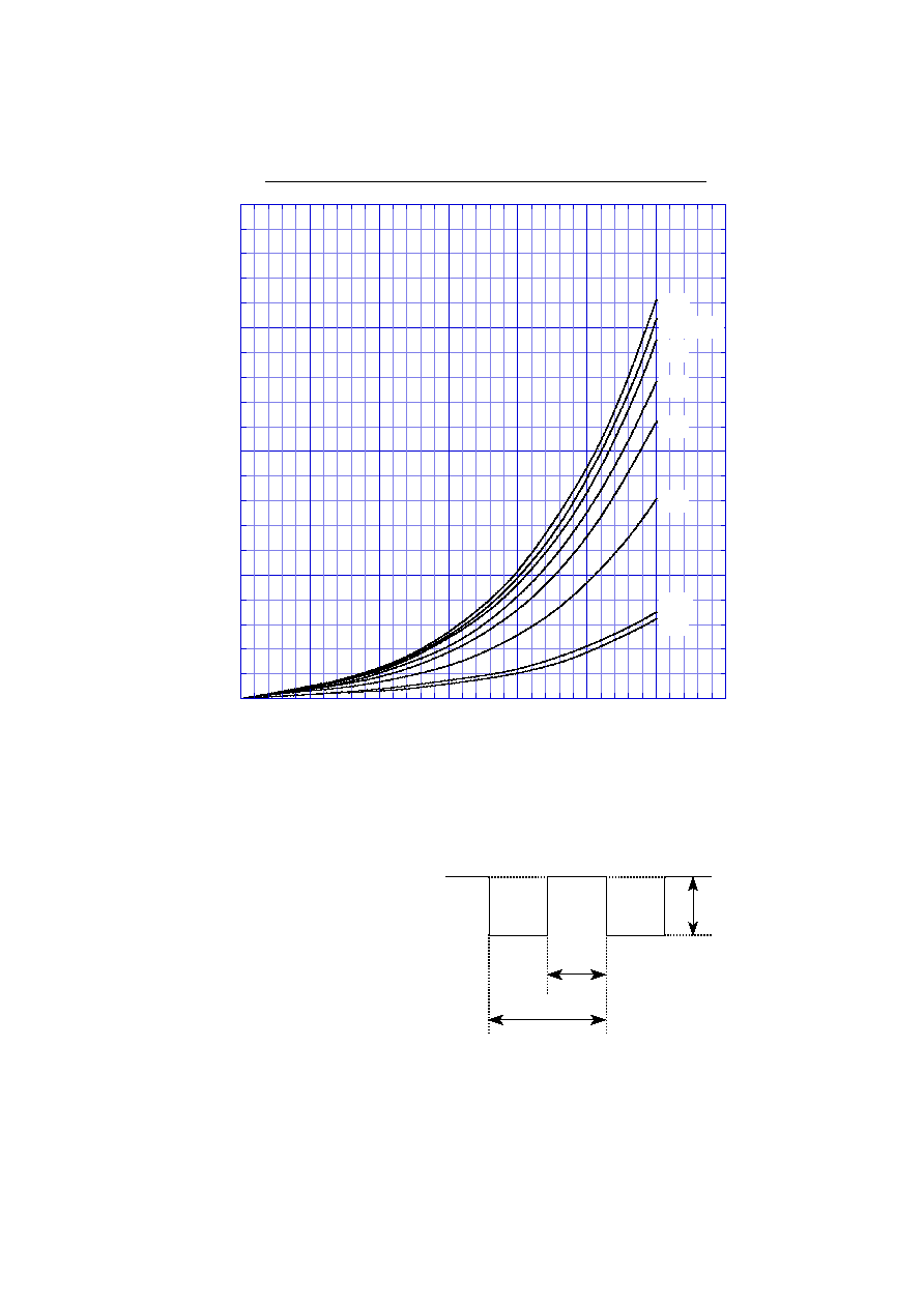
Average Rectified Forward Current
I
O
50Hz sine wave, R-load, Rating for each diode Io/2, Tc=105
40
A
Peak Surge Forward Current
I
FSM
50Hz sine wave, Non-repetitive 1 cycle peak value, Tj=25
350
A
Electrical Characteristics (If not specified Tc=25)
Item
Symbol
Conditions
Ratings
Unit
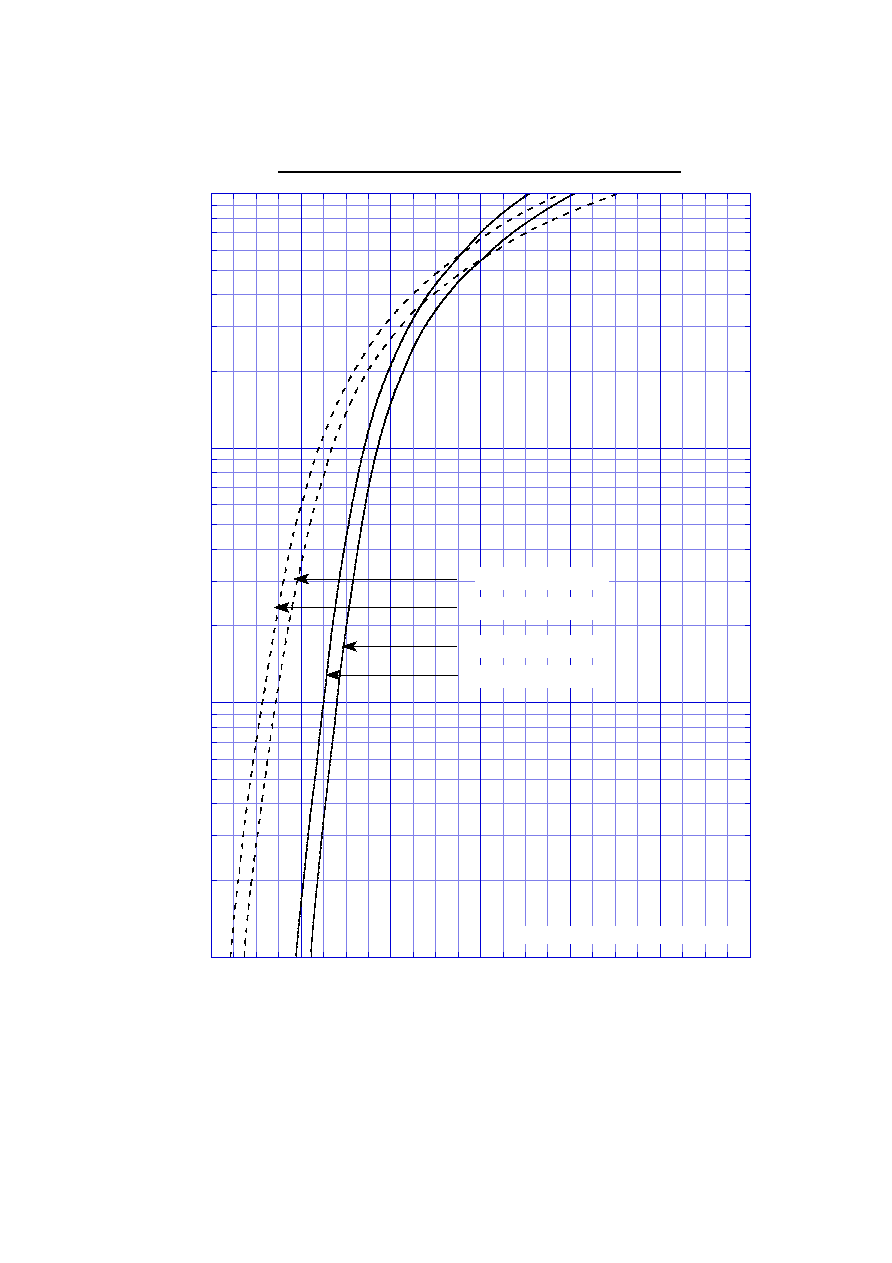
Forward Voltage
V
F
I
F
=15A, Pulse measurement, Rating of per diode
Max.0.4
V
Reverse Current
I
R
V
R
=V
RM
, Pulse measurement, Rating of per diode
Max.45
mA
Junction Capacitance
Cj
f=1MHz, V
R
=10V, Rating of per diode
Typ.1160
pF
Thermal Resistance
jc
junction to case
Max.0.8 /W