DG1H3
30V 1A
Copyright & Copy;2002 Shindengen Electric Mfg.Co.,Ltd.
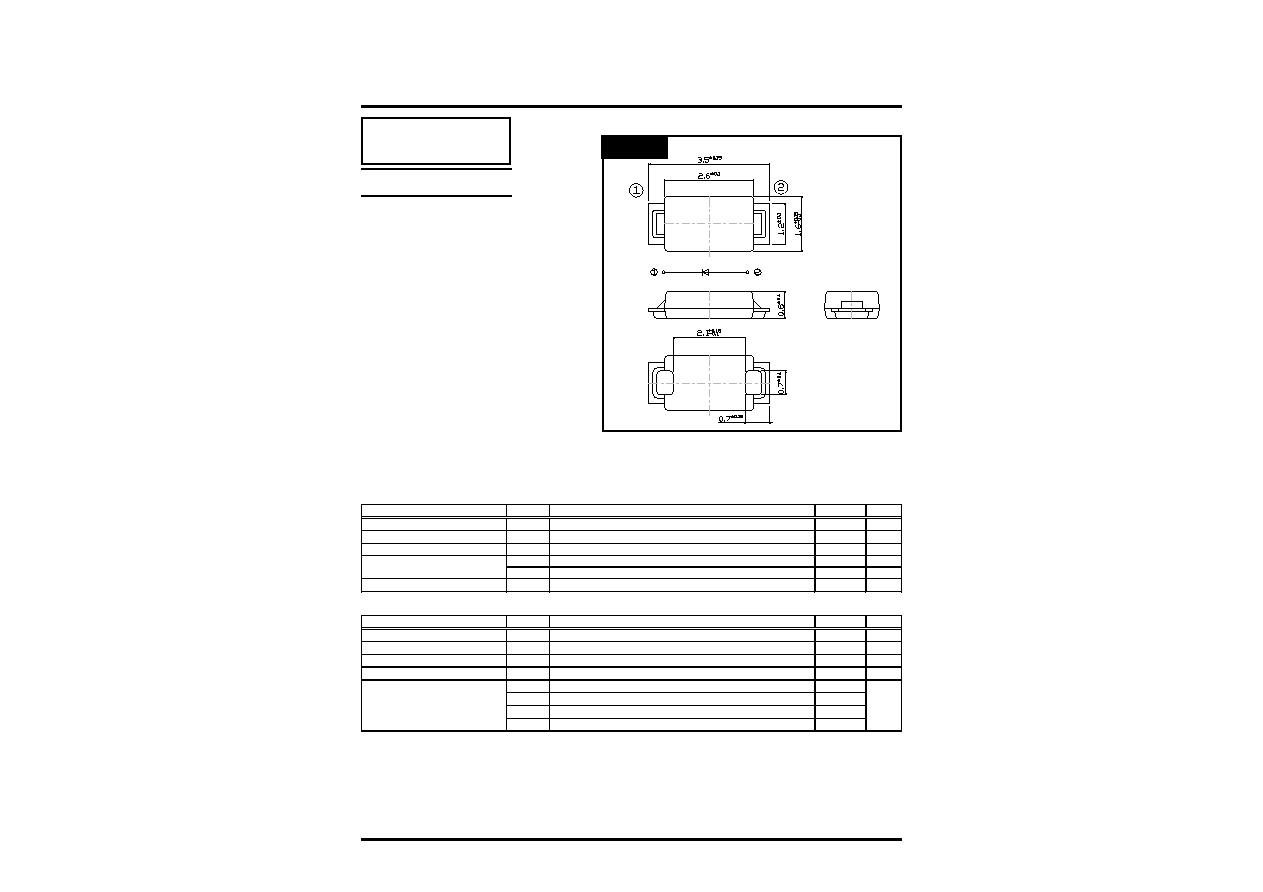
OUTLINE DIMENSIONS
Unit : mm
RATINGS
SHINDENGEN
Case : G1F
Single
Schottky Rectifiers (SBD)
Absolute Maximum Ratings iTl=25 unless otherwise specified)
Item
Symbol
Conditions
Ratings
Unit
Storage Temperature
Tstg
-55 to 125
Operating Junction Temperature
Tj
125
Maximum Reverse Voltage
V
RM
30
V
Average Rectified Forward Current
I
O
50Hz sine wave, R-load, Ta = 26, *1
0.7
A
I
O
50Hz sine wave, R-load, Tl = 113, *3
1.0
A
Peak Surge Forward Current
I
FSM
50Hz sine wave, Non-repetitive 1 cycle peak value, Tj=25
20
A
Electrical Characteristics iTl=25 unless otherwise specified)
Item
Symbol
Conditions
Ratings
Unit
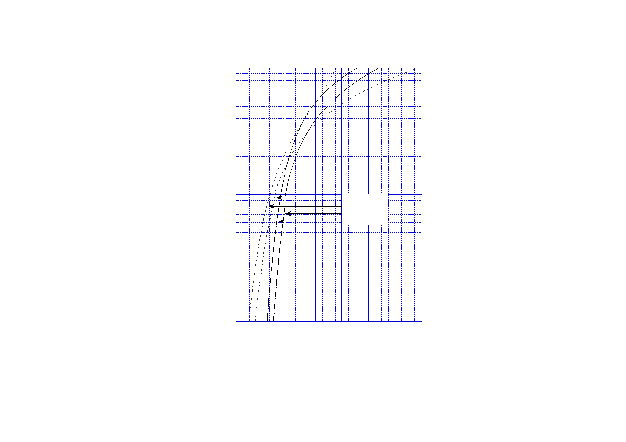
Forward Voltage
V
F
I
F
=0.2A, Pulse measurement
Max 0.30
V
V
F
I
F
=0.7A, Pulse measurement
Max 0.36
V
Reverse Current
I
R
V
R
=V
RM,
Pulse measurement
Max 1
mA
Junction Capacitance
Cj
f=1MHz, V
R
=10V
Typ 37
pF
Æja
junction to ambient, *1
Max 210
Thermal Resistance
Æja
junction to ambient, *2
Max 120
/W
Æja
junction to ambient, *3
Max 70
Æjl
junction to lead, *3
Max 20
*1
Measured on the 1×1 inch phenol substrate (pattern area : 32.6mm
2
)
*2
Measured on the 1×1 inch phenol substrate (pattern area : 160mm
2
)
*3
Measured on the 2×2 inch alumina substrate (pattern area : 2100mm
2
)
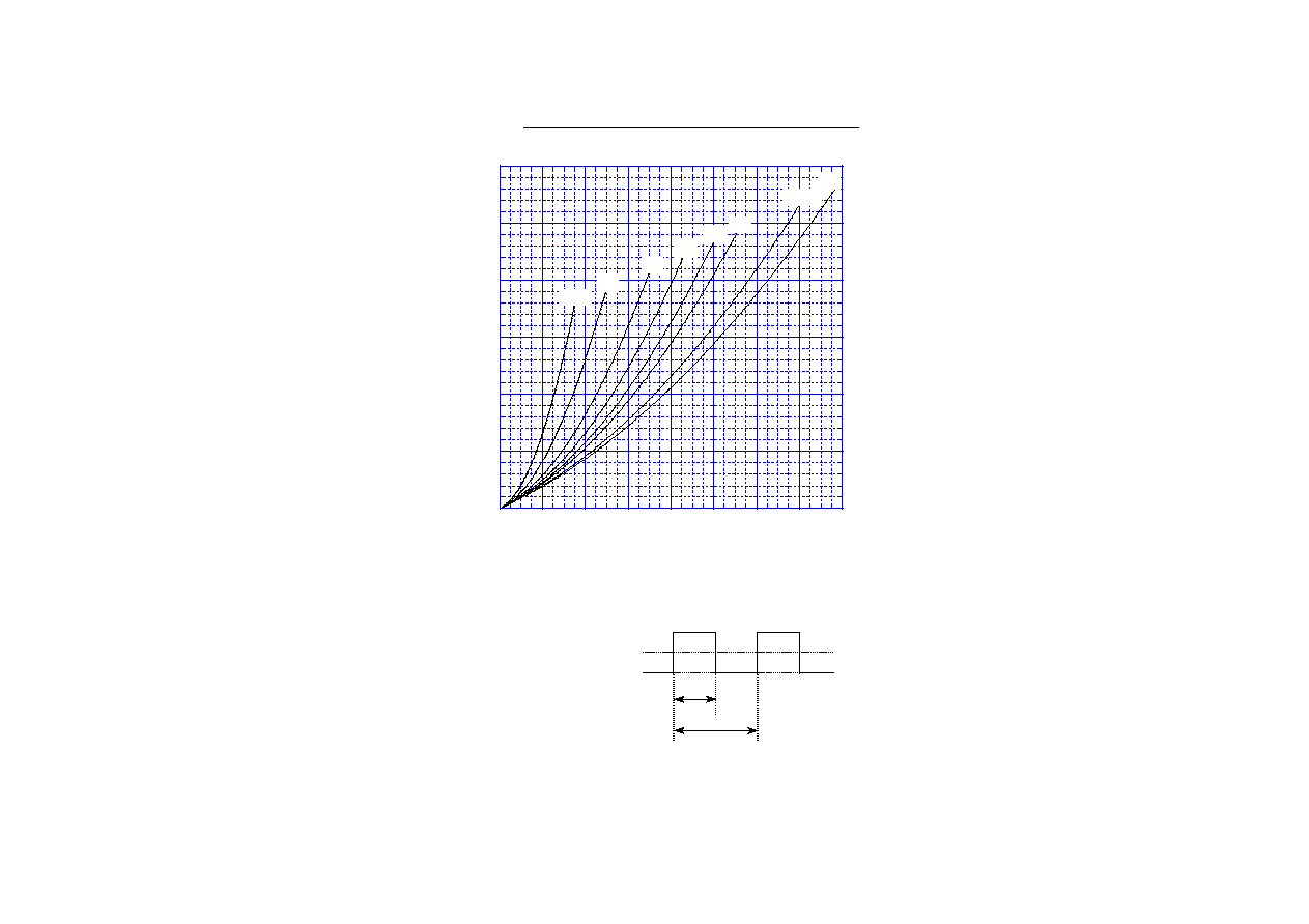
0
5
10
15
20
25
30
1
10
DG1H3
2
5
20
50
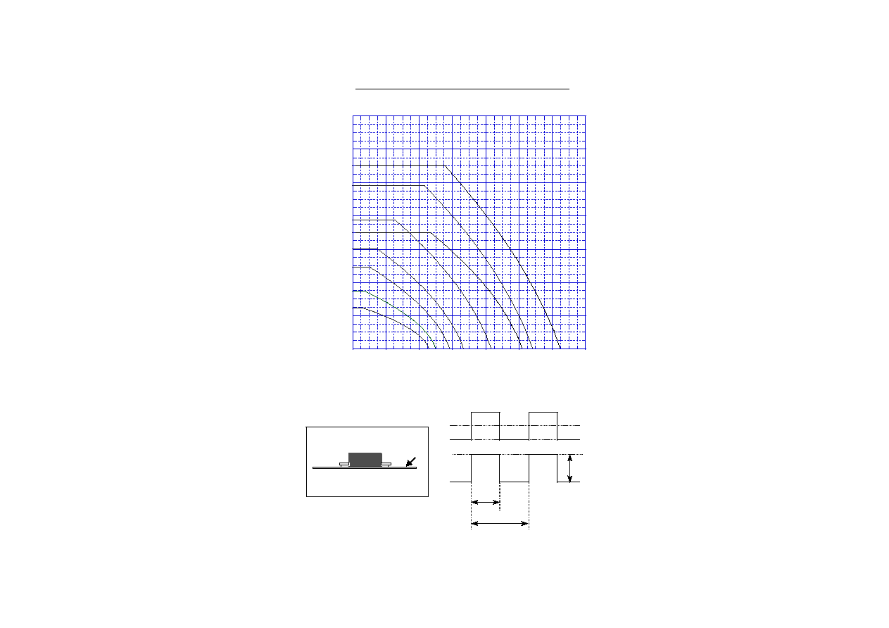
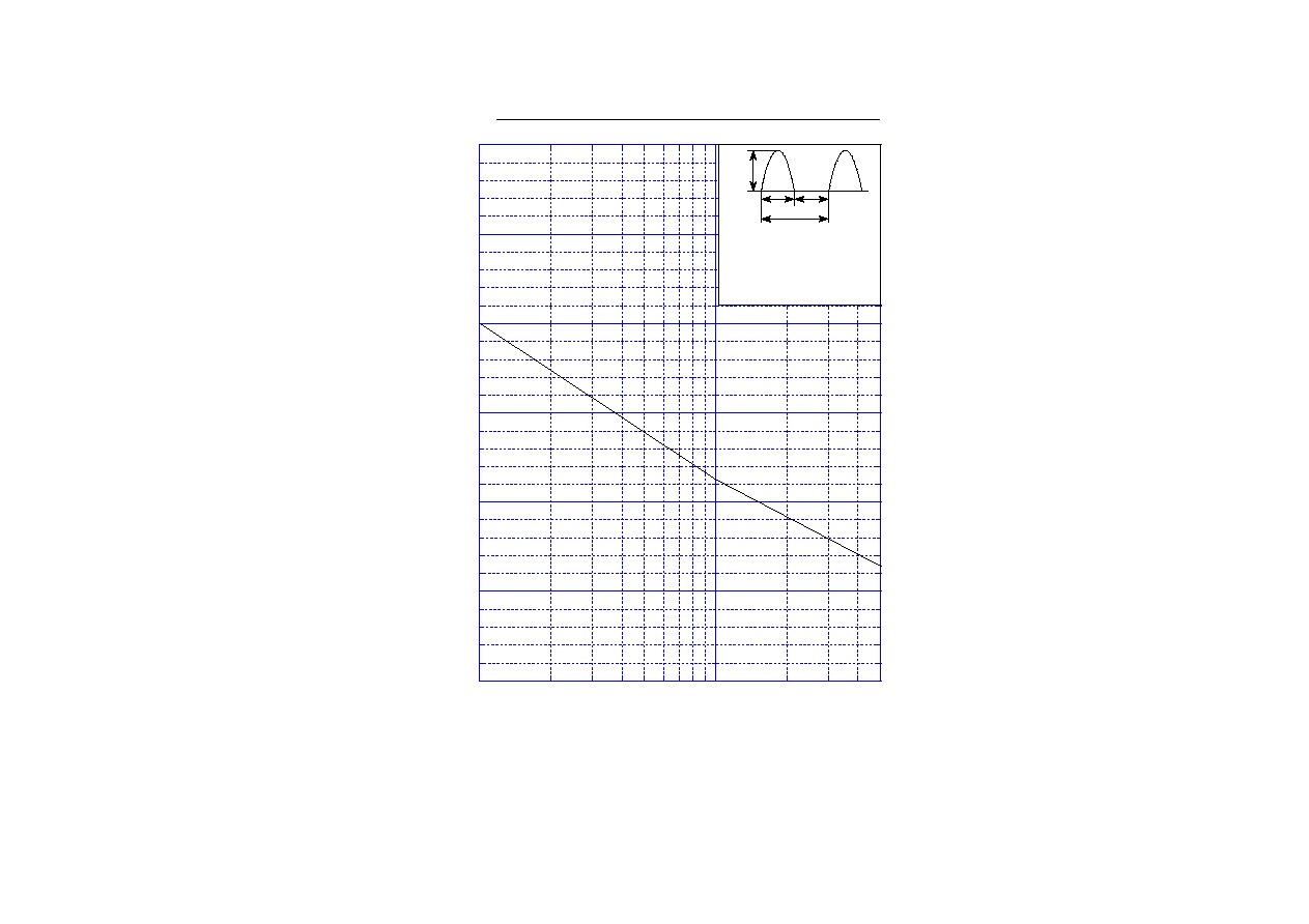
Peak Surge Forward Capability
I
FS
M
[A]
P
eak
S
u
r
g
e F
o
r
w
ar
d
C
u
r
r
e
n
t
Number of Cycles [cycle]
I
FS
M
10ms 10ms
1 cycle
non-repetitive,
sine wave,
Tj=25°C before
surge current is applied