
SPECIFICATIONS
INPUT
Voltage
See Model Selection Table
Max. Input Current
Input
Full Load
Voltage
Input Current
5V
1.1 to 0.6A
12V
0.55 to 0.27A
24V
0.26 to 0.14A
48V
0.15 to 0.07A
OUTPUT
Output Voltage
See Model Selection Table
Set Point
±5%
Regulation
Total
±5% (5% to 100% load change)
Noise & Ripple, (peak-to-peak)
5V Output
100 mV max.
+12V, ±12V Output
120 mV
+15V, ±15V Output
150 mV
Output Current
See Model Selection Table
Short-Circuit Protection
Special constant-current circuit
provides indefinite protection against
overload or short circuit
FEATURES
s
UL1950 Recognized
s
Input-Output Isolation
s
Compact, Single In-Line Package
s
Single and Dual Output
s
Wide-Range Input
s
Input and Output Filters
Insulation Resistance
100 M
at 500 VDC
Dielectric Strength
500 VDC for 1 minute
ENVIRONMENTAL
Operating Ambient
Temp.
≠10 to +70∞C (See Derating Chart)
Storage Temp.
≠30 to +80∞C
1500 VAC Isolation available on some models ≠ consult the factory
1
-
8
0
0
-
6
3
4
-
3
6
5
4
OUTPUT
MODEL AND INPUT RANGE
EFFIC.
VOLTS AMPS 4.0-7.2VDC 8.0-16.5VDC 16-32VDC 28-60VDC
5
0.6
HDF0505S
HDF1205S
HDF2405S HDF4805S 77 - 80%
12
0.26
HDF0512S
HDF1212S
HDF2412S HDF4812S 80 - 85%
15
0.21
HDF0515S
HDF1215S
HDF2415S HDF4815S 80 - 85%
±12
0.125 HDF0512D
HDF1212D HDF2412D HDF4812D 74 - 77%
±15
0.1
HDF0515D
HDF1215D HDF2415D HDF4815D 74 - 77%
MODEL SPECIFICATIONS
DERATING CHART
3 Watt
HD Series
Watts
1
0
≠30
≠10
50
70 80
2
3
HDF12XX, HDF24XX
+
IN
≠
Input
Capacitor
Power
Switching
Circuit
Feed back
Dual Output Type
Input
Voltage
Monitoring
Cicuit
Control
Circuit
3 Terminals
Voltage Reg.
Switching
Circuit
OUT
COM
+
≠
Output
Voltage
Detector
Cicuit
BLOCK DIAGRAM
1
-
8
0
0
-
6
3
4
-
3
6
5
4
3 Watt
HD Series
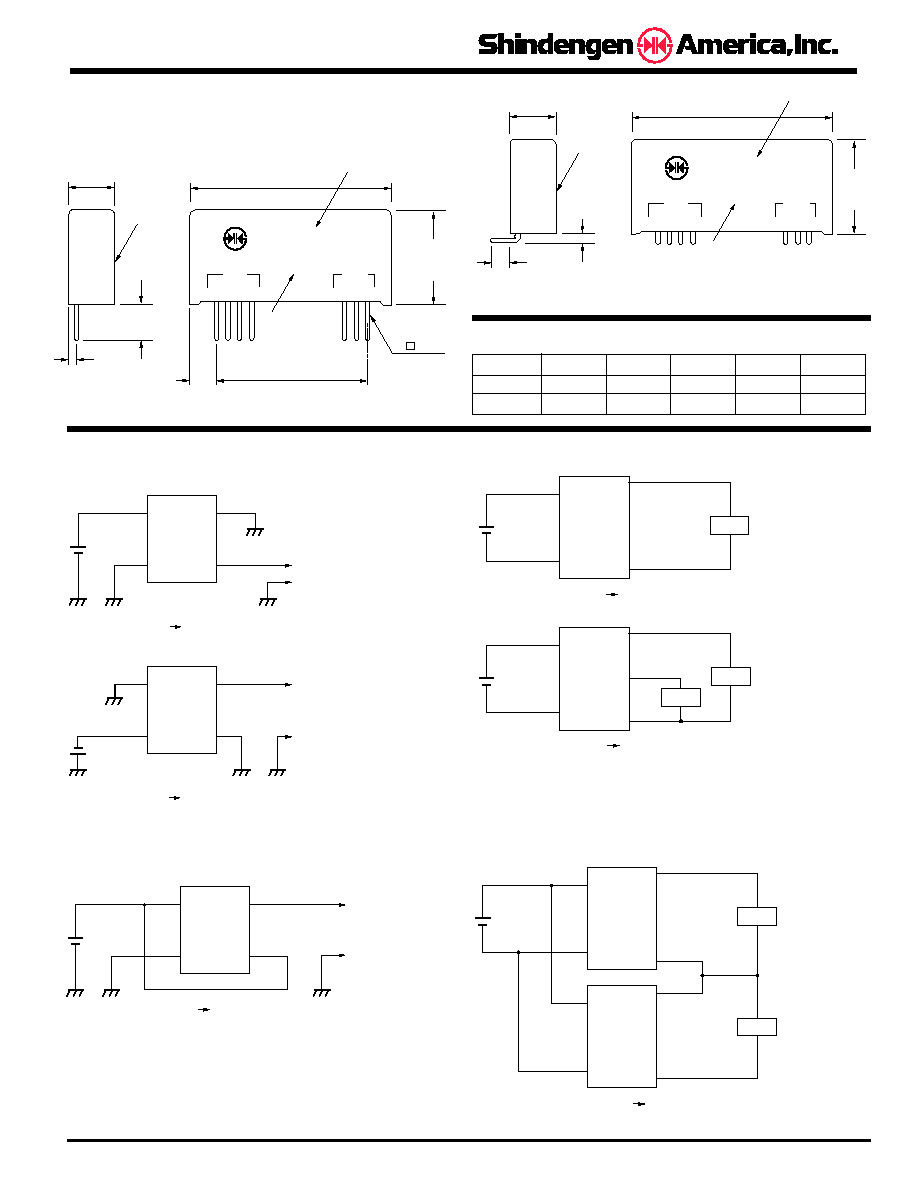
MECHANICAL SPECIFICATIONS
Size (W x D x H) 1.75 x 0.81 x 0.43" (44.5 x 20.5 x 10.5 mm)
Weight 0.6 oz (16 g)
1.76
(44.5)
0.81
(20.5)
HDF≠0512D
0.09
(2.29)
13 X 0.10 = 1.3
(13 X 2.54 = 33.02)
1
2
3
4
5
6
7
Date Code
Model No.
1401
IN OUT
+ + ≠ ≠ + o ≠
0.44
(10.5)
0.23 ±0.02
(5.84)
Face
0.25 ±0.04
(6.35)
7- 0.025
(0.64)
M d l N
PIN # 1 2 3 4, 5 6, 7
FUNCTION-D OUT
≠
COM OUT
+
IN
≠
IN
+
FUNCTION-S NC OUT
≠
OUT
+
IN
≠
IN
+
PIN DESCRIPTION
Dimensions in inches; ( ) Dimensions in mm.
1
1.76
(44.5)
0.81
(20.5)
HDF≠0512D
0.24 ±0.04
(6.1)
2
3
4
5
6
7
Date Code
Model No.
1401
IN OUT
+ + ≠ ≠ + o ≠
0.44
(10.5)
Face
0.08 ±0.02
(2.03)
-
5V
+
5V
HDF
-0505
IN
:
+
5V OUT: ≠5V
IN
+
OUT
+
OUT
≠
IN
≠
-
5V
+
5V
HDF
-0505
IN
: ≠5V OUT:
+
5V
IN
+
OUT
+
OUT
≠
IN
≠
+
10V
+
5V
HDF
-0505
IN
:
+
5V OUT:
+
10V
IN
+
OUT
+
OUT
≠
IN
≠
+
5V
HDF
-0512
IN
:
+
5V OUT:
+
24V
IN
+
OUT
+
OUT
≠
IN
≠
+
5V
Load
G
+
5V
HDF
-0512
IN
:
+
5V OUT:
+
12V,
+
24V
IN
+
OUT
+
OUT
≠
COM
IN
≠
+
5V
+
12V
Load
G
Load
+
5V
HDF
-0512
IN
:
+
5V OUT:
±
24V
IN
+
OUT
+
OUT
≠
IN
≠
HDF
-0512
IN
+
OUT
+
OUT
≠
IN
≠
+
24V
--24V
Load
Load
G
APPLICATION EXAMPLES
1. Reverse Polarity Output
3. Series Connection of Dual Output modules
2. Series Connection of Output with Input
4. Series Connection of Two or More Units
s
The output current capacity is the same as the output current
capacity of the converter. (For example, an HDF-0505 connected
as shown above has an output rating of 10 VDC at 600 mA.
s
The combined output regulation is:
(Output regulation of HDF-0505) + (Input Voltage Fluctuation)
s
Because the current output from the OUT-terminal is the sum of
the +24V and the +12V outputs, this value must not exceed the
rated output current. In the HDF-0512D, this value is 125 mA.
With optional formed leads available - use "-F suffix."