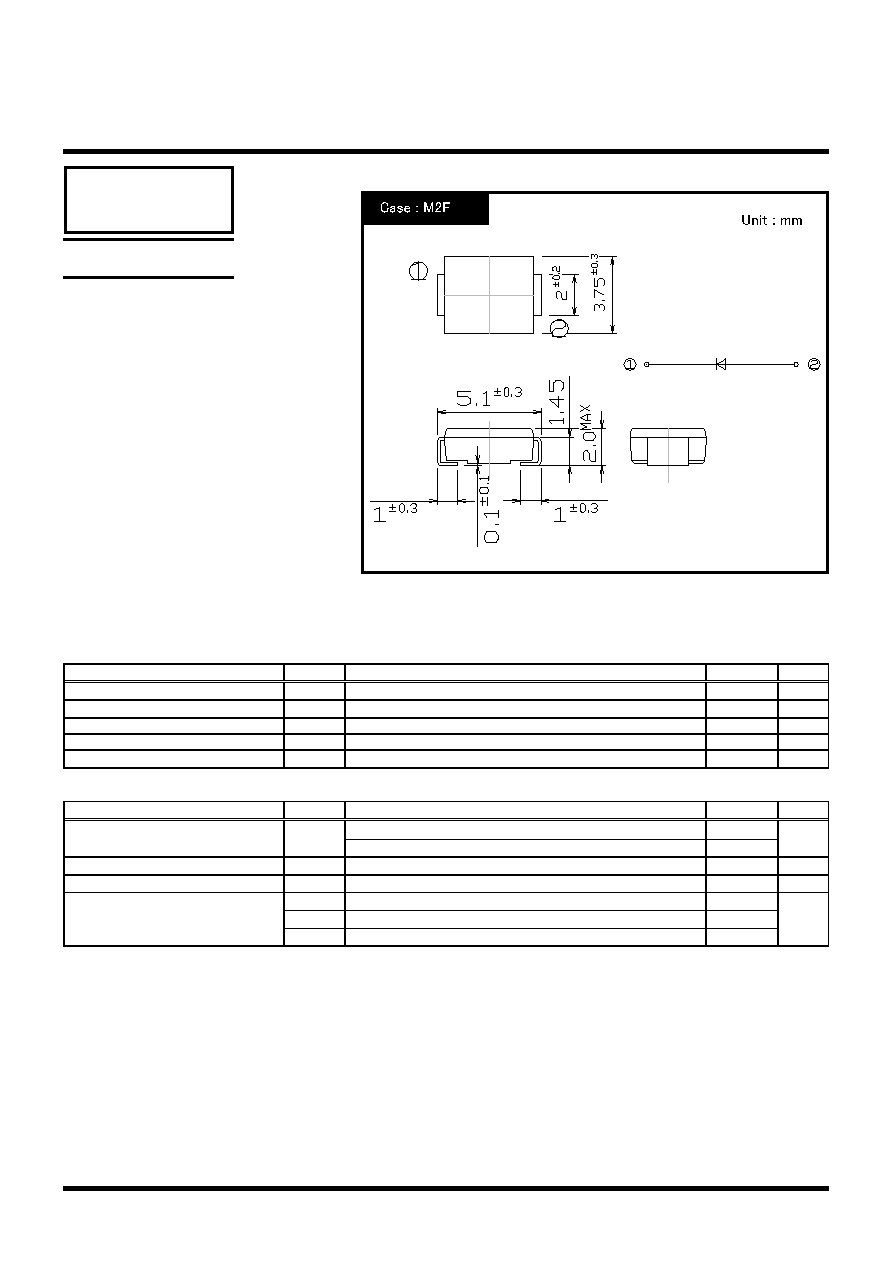
M2FH3
30V 6A
Copyright & Copy;2000 Shindengen Electric Mfg.Co.Ltd
OUTLINE DIMENSIONS
RATINGS
SHINDENGEN
Single
Schottky Rectifiers (SBD)
Absolute Maximum Ratings (If not specified, Tc=25)
Item
Symbol
Conditions
Ratings
Unit
Storage Temperature
Tstg
-55`125
Operating Junction Temperature
T
j
125
Maximum Reverse Voltage
V
RM
30
V
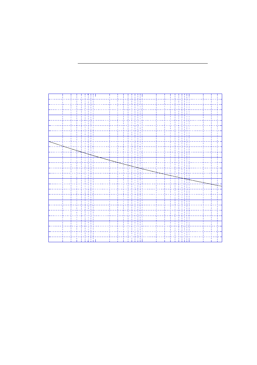
Average Rectified Forward Current
I
O
50Hz sine wave, R-load Tc=70 On glass-epoxy substrate
6
A
Peak Surge Forward Current
I
FSM
50Hz sine wave, Non-repetitive 1 cycle peak value, Tj=25
110
A
Electrical Characteristics iIf not specified, Tc=25j
Item
Symbol
Conditions
Ratings
Unit
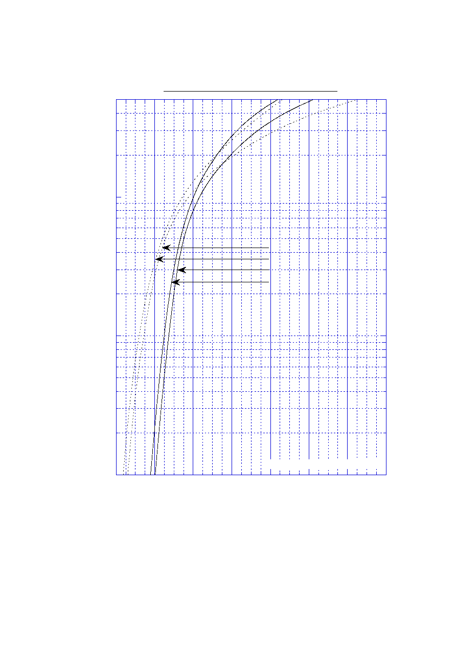
Forward Voltage
V
F
I
F
=2.0A, Pulse measurement
Max.0.30
V
I
F
=6.0A, Pulse measurement
Max.0.36
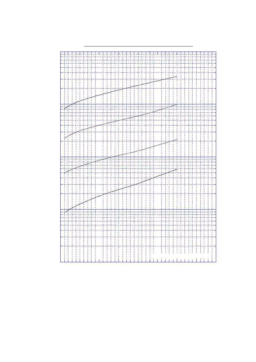
Reverse Current
I
R
V
R
=30V, Pulse measurement
Max.4.0
mA
Junction Capacitance
Cj
f=1MHz, V
R
=10V
Typ.240
pF
∆jc
junction to case
Max.14
Thermal Resistance
∆jl
junction to lead
Max.16
/W
∆ja
junction to ambient On glass-epoxy substrate
Max.55
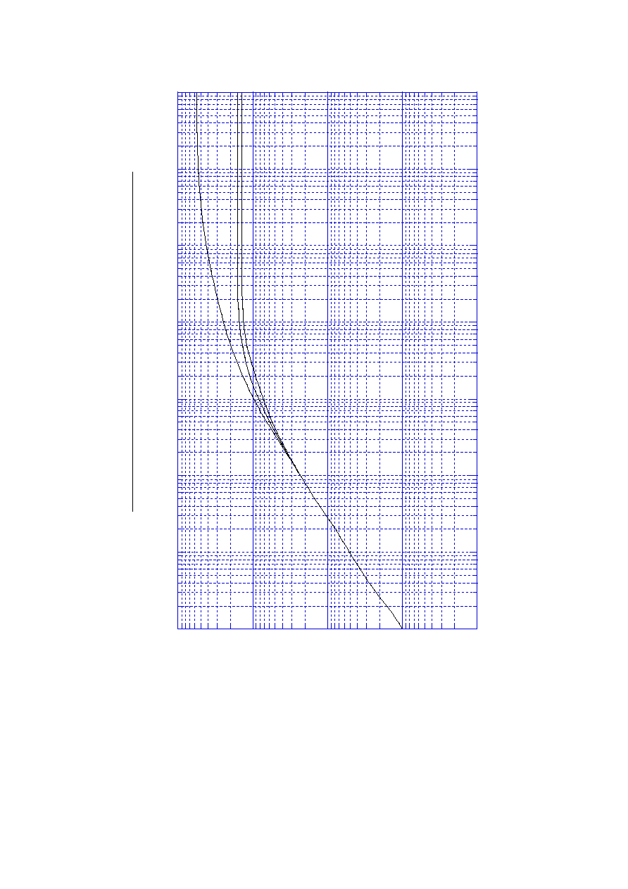
0
20
40
60
80
100
120
140
160
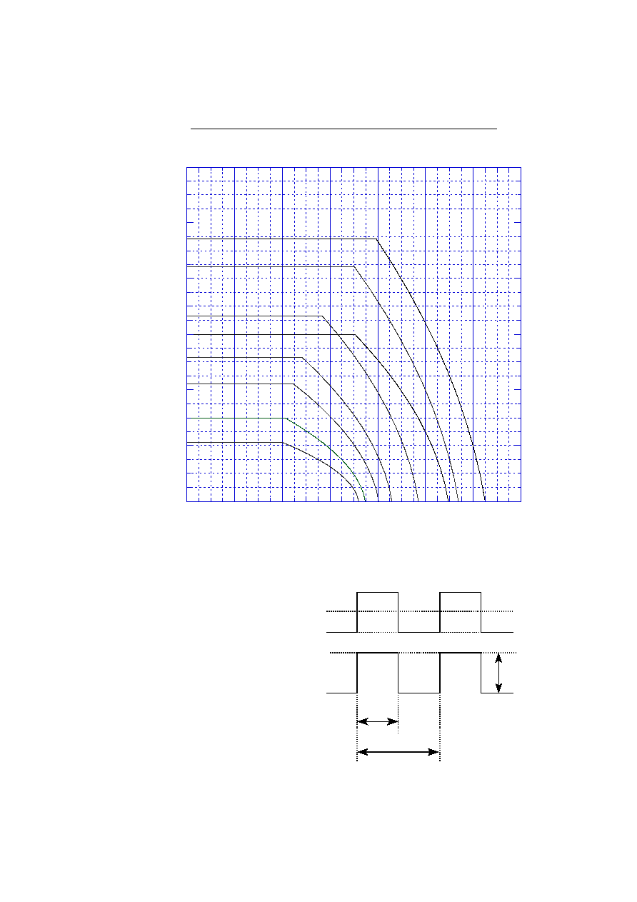
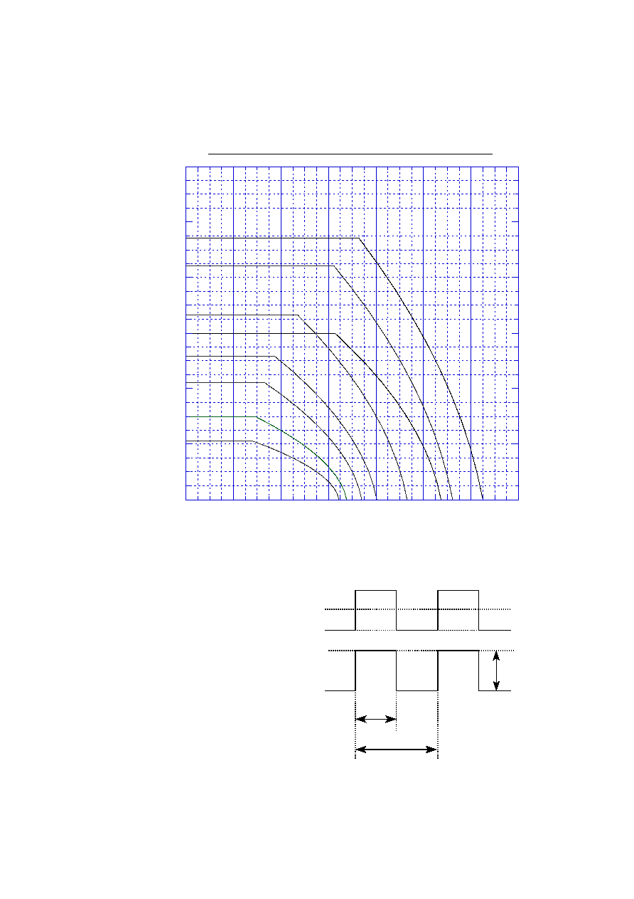
1
10
100
2
5
20
50
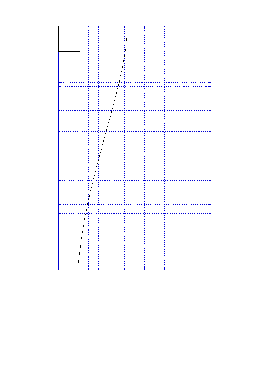
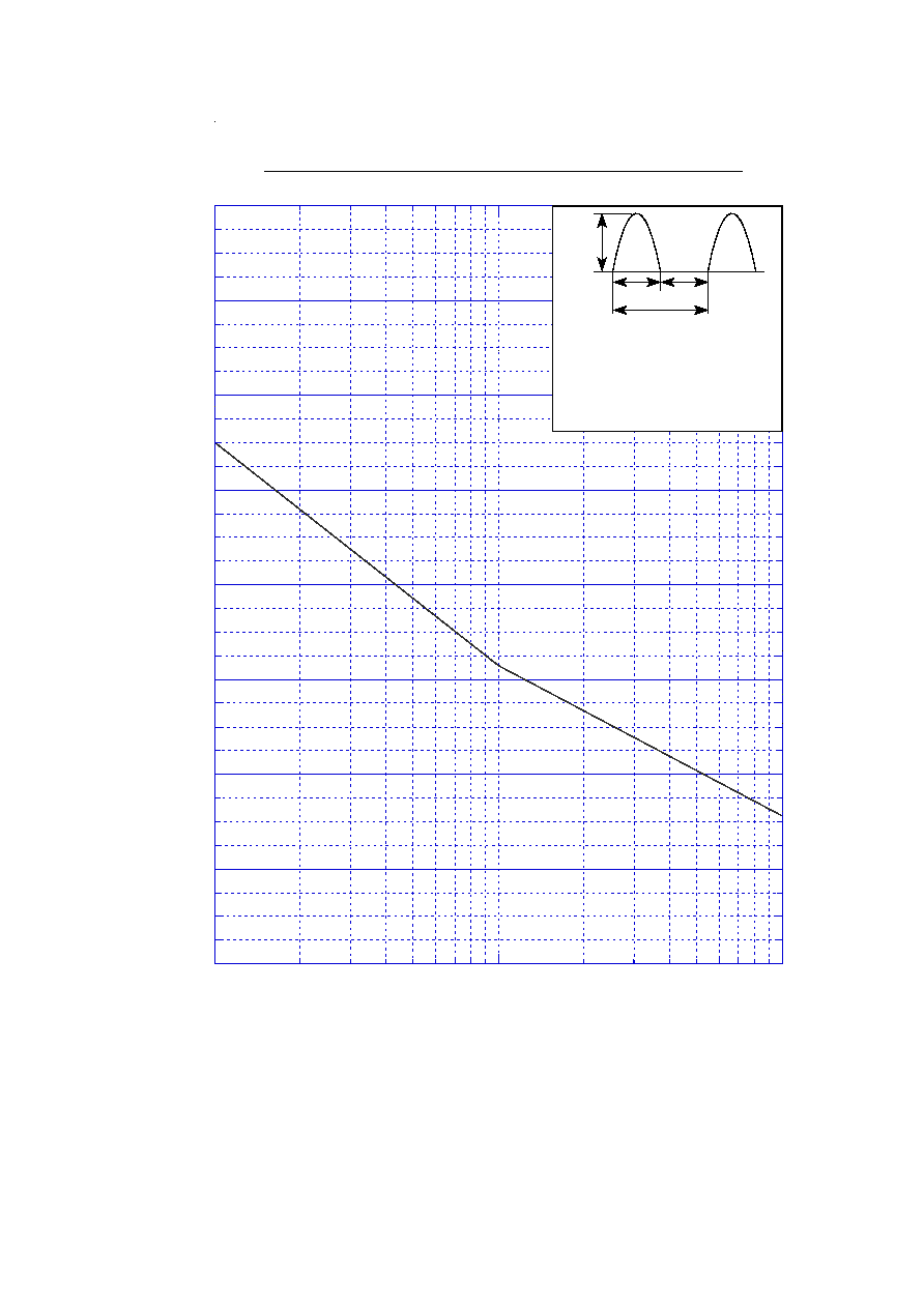
M2FH3
I
FSM
10ms 10ms
1 cycle
non-repetitive,
sine wave,
Tj=25∞C before
surge current is applied
Peak Surge Forward Capability
Number of Cycles [cycle]
Peak Surge Forw
ard Current I
FSM
[A]