NPN Silicon RF Transistor
BFQ 82
ESD: Electrostatic discharge sensitive device, observe handling precautions!
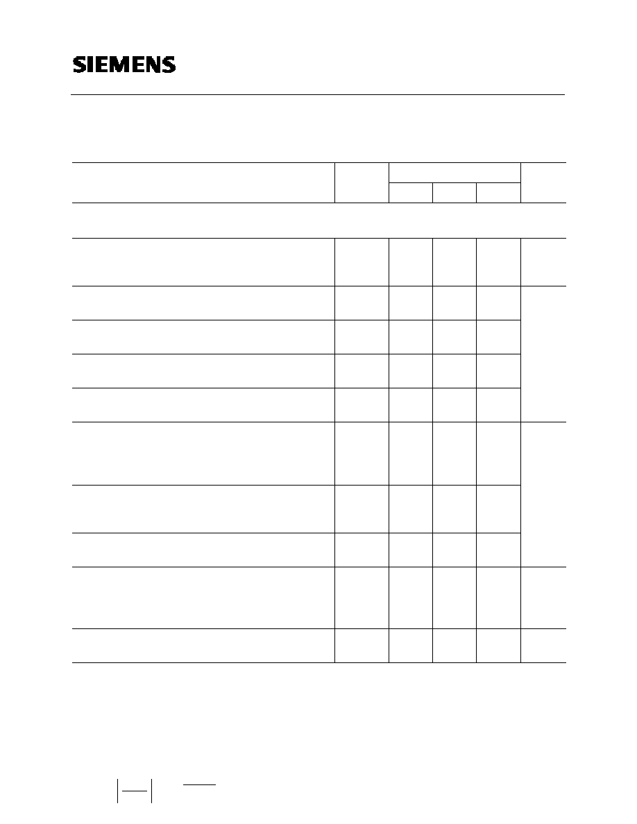
Maximum Ratings
Type
Marking
Package
1)
Pin Configuration
BFQ 82
Q62702-F1189
82
Cerec-X
1
2
3
4
B
E
C
E
Ordering Code
(tape and reel)
Parameter
Symbol
Values
Unit
Collector-emitter voltage
V
CE0
12
V
Emitter-base voltage
V
EB0
2
Collector current
I
C
80
mA
Collector-base voltage
V
CB0
20
Base current
I
B
10
Junction temperature
T
j
175
∞C
Ambient temperature range
T
A
≠ 65 ... + 175
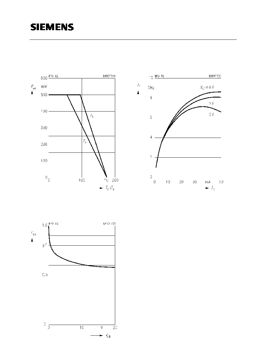
Total power dissipation,
T
S
95 ∞C
3)
P
tot
500
mW
Storage temperature range
T
stg
≠ 65 ... + 175
Thermal Resistance
Junction - ambient
2)
R
th JA
240
K/W
Junction - case
3)
R
th JS
160
Collector-emitter voltage,
V
BE
= 0
V
CES
20
Peak collector current,
f
10 MHz
I
CM
80
Peak base current,
f
10 MHz
I
BM
10
1)
For detailed information see chapter Package Outlines.
2)
Package mounted on alumina 15 mm
◊
16.7 mm
◊
0.7 mm.
3)
T
S
is measured on the collector lead at the soldering point to the pcb.
q
For low-noise, high-gain amplifiers up to 2 GHz.
q
Linear broadband applications at collector currents
up to 40 mA.
q
Hermetically sealed ceramic package.
q
f
T
= 8 GHz
F
= 1.1 dB at 800 MHz

Electrical Characteristics
at
T
A
= 25 ∞C, unless otherwise specified.
Unit
Values
Parameter
Symbol
min.
typ.
max.
DC Characteristics
V
Collector-emitter breakdown voltage
I
C
= 1 mA,
I
B
= 0
V
(BR)CE0
12
≠
≠
Collector-base cutoff current
V
CB
= 10 V,
I
E
= 0
V
CB
= 10 V,
I
E
= 0
, T
A
= 125 ∞C
I
CB0
≠
≠
≠
≠
0.05
5
µ
A
Collector-emitter cutoff current
V
CE
= 20 V,
V
BE
= 0
I
CES
≠
≠
100
Emitter-base cutoff current
V
EB
= 1 V,
I
C
= 0
I
EB0
≠
≠
1
≠
DC current gain
I
C
= 5 mA,
V
CE
= 8 V
I
C
= 30 mA,
V
CE
= 8 V
h
FE
≠
50
110
120
≠
250
BFQ 82
Electrical Characteristics
at
T
A
= 25 ∞C, unless otherwise specified.
AC Characteristics
Unit
Values
Parameter
Symbol
min.
typ.
max.
Power gain
I
C
= 30 mA,
V
CE
= 8 V,
f
= 1 GHz,
Z
0
= 50
I
C
= 30 mA,
V
CE
= 8 V,
f
= 2 GHz,
Z
0
= 50
G
ma
1)
≠
≠
17
11
≠
≠
GHz
Transition frequency
I
C
= 5 mA,
V
CE
= 8 V,
f
= 500 MHz
I
C
= 30 mA,
V
CE
= 8 V,
f
= 500 MHz
f
T
≠
≠
3.6
8
≠
≠
Collector-emitter capacitance
V
CE
= 10 V,
V
BE
=
v
be
= 0,
f
= 1 MHz
C
ce
≠
0.4
≠
Output capacitance
V
CE
= 10 V,
V
BE
=
v
be
= 0,
f
= 1 MHz
C
obs
≠
1.0
≠
dB
Noise figure
I
C
= 5 mA,
V
CE
= 8 V,
f
= 10 MHz,
Z
S
= 75
I
C
= 30 mA,
V
CE
= 8 V,
f
= 800 MHz,
Z
S
=
Z
Sopt
I
C
= 10 mA,
V
CE
= 8 V,
f
= 2 GHz,
Z
S
=
Z
Sopt
F
≠
≠
≠
0.7
1.6
2.3
≠
≠
≠
pF
Collector-base capacitance
V
CB
= 10 V,
V
BE
=
v
be
= 0,
f
= 1 MHz
C
cb
≠
0.62
≠
Input capacitance
V
EB
= 0.5 V,
I
C
=
i
c
= 0,
f
= 1 MHz
C
ibo
≠
2.5
≠
Transducer gain
I
C
= 30 mA,
V
CE
= 8 V,
f
= 1 GHz,
Z
0
= 50
I
S
21e
I
2
≠
13.5
≠
mV
Linear output voltage
two-tone intermodulation test
I
C
= 40 mA,
V
CE
= 8 V,
d
IM
= 60 dB,
f
1
= 806 MHz,
f
2
= 810 MHz,
Z
S
=
Z
L
= 50
V
o1
=
V
o2
≠
280
≠
dBm
Third order intercept point
I
C
= 40 mA,
V
CE
= 8 V,
f
= 800 MHz
IP
3
≠
32
≠
1)
S
21e
S
12e
(k ≠
k
2
≠ 1)
BFQ 82