 | –≠–ª–µ–∫—Ç—Ä–æ–Ω–Ω—ã–π –∫–æ–º–ø–æ–Ω–µ–Ω—Ç: C509-L | –°–∫–∞—á–∞—Ç—å:  PDF PDF  ZIP ZIP |

Data Sheet 09.96
Microcomputer Components
C509-L
8-Bit CMOS Microcontroller

Semiconductor Group
1
09.96
C509-L
8-Bit CMOS Microcontroller
Advance Information
C509-L
∑
Full upward compatibility with SAB 80C517/80C517A and 8051/C501 microcontrollers
∑
256 byte on-chip RAM
∑
3K byte of on-chip XRAM
∑
256 directly addressable bits
∑
375 ns instruction cycle at 16-MHz oscillator frequency
∑
On-chip emulation support logic (Enhanced Hooks Technology
TM
)
∑
External program and data memory expandable up to 64 Kbyte each
∑
8-bit A/D converter with 15 multiplexed inputs and built-in self calibration
∑
Two 16-bit timers/counters (8051 compatible)
∑
Three 16-bit timers/counters (can be used in combination with the compare/capture unit)
∑
Powerful compare/capture unit (CCU) with up to 29 high-speed or PWM output channels or 13
capture inputs
∑
Arithmetic unit for division, multiplication, shift and normalize operations
∑
Eight datapointers instead of one for indirect addressing of program and external data memory
(further features are on next page)
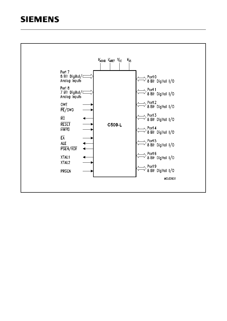
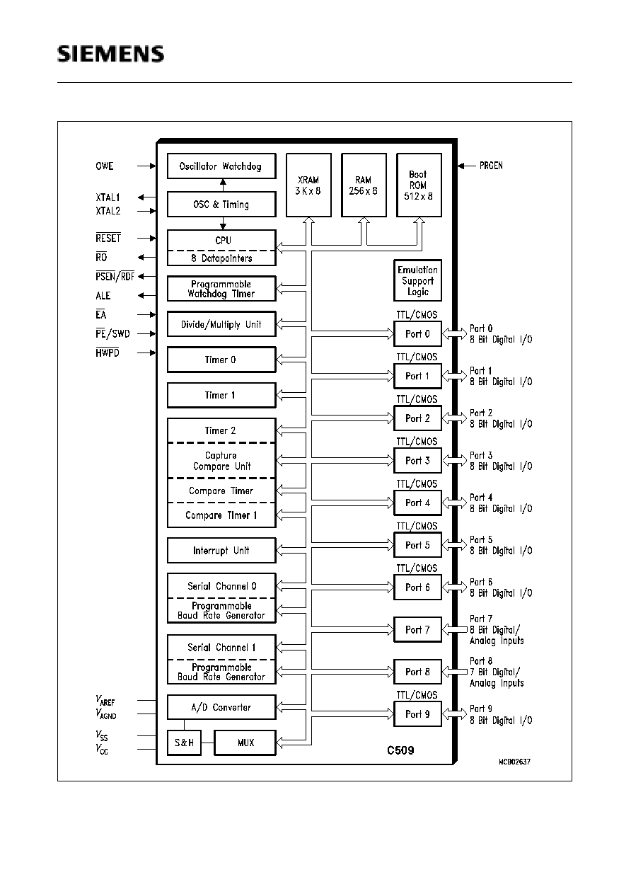
Figure 1
C509-L Functional Units

C509-L
Semiconductor Group
2
Features (continued) :
∑
Extended watchdog facilities
≠ 15-bit programmable watchdog timer
≠ Oscillator watchdog
∑
Ten I/O ports
≠ Eight bidirectional 8-bit I/O ports with selectable port structure
quasi-bidirectional port structure (8051 compatible)
bidirectional port structure with CMOS voltage levels
≠ One 8-bit and one 7-bit input port for analog and digital input signals
∑
Two full-duplex serial interfaces with own baud rate generators
∑
Four priority level interrupt systems, 19 interrupt vectors
∑
Three power saving modes
≠ Slow-down mode
≠ Idle mode
≠ Power-down mode
∑
Siemens high-performance ACMOS technology
∑
M-QFP-100-2 rectangular quad flat package
∑
Temperature Ranges :
SAB-C509-L
T
A
= 0 to 70
∞
C
SAF-C509-L
T
A
= -40 to 85
∞
C
The C509-L is a high-end microcontroller in the Siemens C500 8-bit microcontroller family. lt is
based on the well-known industry standard 8051 architecture; a great number of enhancements
and new peripheral features extend its capabilities to meet the extensive requirements of new
applications. Further, the C509-L is a superset of the Siemens SAB 80C517/80C517A 8-bit
microcontroller thus offering an easy upgrade path for SAB 80C517/80C517A users.
The high performance of the C509-L microcontroller is achieved by the C500-Core with a maximum
operating frequency of 16 MHz internal (and external) CPU clock. While maintaining all the features
of the SAB 80C517A, the C509-L is expanded by one I/O port, in its compare/capture capabilities,
by A/D converter functions, by additional 1 KByte of on-chip RAM (now 3 KByte XRAM) and by an
additional user-selectable CMOS port structure. The C509-L is mounted in a P-MQFP-100-2
package.
Note: Versions for extended temperature ranges ≠ 40 ∞C to 110 ∞C (SAH-C509-L) and ≠ 40 ∞C to
125 ∞C (SAK-C509-L) are available on request.
Ordering Information
Type Ordering
Code
Package
Description
(8-Bit CMOS microcontroller)
SAB-C509-LM
Q67120-C1045
P-MQFP-100-2
for external memory (16 MHz)
SAF-C509-LM
Q67120-C0983
P-MQFP-100-2
for external memory (16 MHz)
ext. temp. ≠ 40 ∞C to 85 ∞C
Semiconductor Group
3
09.96
C509-L
Figure 2
Logic Symbol
C509-L
Semiconductor Group
4
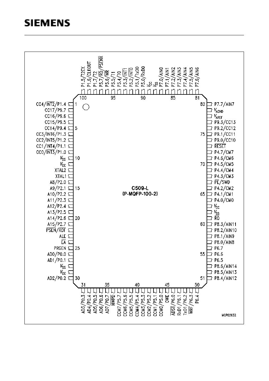
Figure 3
C509-L Pin Configuration (P-MQFP-100-2, Top View)
Semiconductor Group
5
09.96
C509-L
Table 1
Pin Definitions and Functions
Symbol
Pin Number
I/O*)
Function
P1.0 - P1.7
9-6, 1,
100-98
9
8
7
6
1
100
99
98
I/O
Port 1
is an 8-bit quasi-bidirectional I/O port with internal pullup
resistors. Port 1 pins that have 1's written to them are
pulled high by the internal pullup resistors, and in that
state can be used as inputs. As inputs, port 1 pins being
externally pulled low will source current (
I
IL
, in the DC
characteristics) because of the internal pullup resistors.
Port 1 can also be switched into a bidirectional mode, in
which CMOS levels are provided. In this bidirectional
mode, each port 1 pin can be programmed individually
as input or output.
Port 1 also contains the interrupt, timer, clock, capture
and compare pins that are used by various options. The
output latch corresponding to a secondary function must
be programmed to a one (1) for that function to operate
(except when used for the compare functions).
The secondary functions are assigned to the pins of
port 1 as follows :
P1.0
INT3 CC0
Interrupt 3 input / compare 0 output /
capture 0 input
P1.1
INT4 CC1
Interrupt 4 input / compare 1 output /
capture 1 input
P1.2
INT5 CC2
Interrupt 5 input / compare 2 output /
capture 2 input
P1.3
INT6 CC3
Interrupt 6 input / compare 3 output /
capture 3 input
P1.4
INT2 CC4
Interrupt 2 input / compare 4 output /
capture 4 input
P1.5
T2EX
Timer 2 external reload trigger input
P1.6
CLKOUT
System clock output
P1.7
T2
Counter 2 input
*) I = Input
O = Output

C509-L
Semiconductor Group
6
P9.0 - P9.7
74-77,
5-2
I/O
Port 9
is an 8-bit quasi-bidirectional I/O port with internal pullup
resistors. Port 9 pins that have 1's written to them are
pulled high by the internal pullup resistors, and in that
state can be used as inputs. As inputs, port 9 pins being
externally pulled low will source current (
I
IL
, in the DC
characteristics) because of the internal pullup resistors.
Port 9 can also be switched into a bidirectional mode, in
which CMOS levels are provided. In this bidirectional
mode, each port 1 pin can be programmed individually
as input or output.
Port 9 also serves alternate compare functions. The out-
put latch corresponding to a secondary function must be
programmed to a one (1) for that function to operate.
The secondary functions are assigned to the pins of
port 9 as follows :
P9.0-P9.7 CC10-CC17
Compare/capture channel 0-7
output/input
XTAL2
12
≠
XTAL2
is the input to the inverting oscillator amplifier and input
to the internal clock generator circuits.
When supplying the C509-L with an external clock
source, XTAL2 should be driven, while XTAL1 is left
unconnected. A duty cycle of 0.4 to 0.6 of the clock
signal is required. Minimum and maximum high and low
times as well as rise/fall times specified in the AC
characteristics must be observed.
XTAL1
13
≠
XTAL1
Output of the inverting oscillator amplifier. This pin is
used for the oscillator operation with crystal or ceramic
resonartor
*) I = Input
O = Output
Table 1
Pin Definitions and Functions (cont'd)
Symbol
Pin Number
I/O*)
Function
Semiconductor Group
7
09.96
C509-L
P2.0 ≠ P2.7
14-21
I/O
Port 2
is a 8-bit I/O port. Port 2 emits the high-order address
byte during fetches from external program memory and
during accesses to external data memory that use 16-bit
addresses (MOVX @DPTR). In this application it uses
strong internal pullup resistors when issuing 1s. During
accesses to external data memory that use 8-bit
addresses (MOVX @Ri), port 2 issues the contents of the
P2 special function register.
P2.0 - P2.7
A8 - A15
Address lines 8 - 15
PSEN / RDF
22
O
Program Store Enable / Read FLASH
The PSEN output is a control signal that enables the
external program memory to the bus during external
code fetch operations. It is activated every third
oscillator period. PSEN is not activated during external
data memory accesses caused by MOVX instructions.
PSEN is not activated when instructions are executed
from the internal Boot ROM or from the XRAM.
In external programming mode RDF becomes active
when executing external data memory read (MOVX)
instructions.
ALE
23
O
Address Latch Enable
This output is used for latching the low byte of the
address into external memory during normal operation.
It is activated every third oscillator period except during
an external data memory access caused by MOVX
instructions.
EA
24
I
External Access Enable
The status of this pin is latched at the end of a reset.
When held at low level, the C509-L fetches all
instructions from the external program memory. For the
C509-L this pin must be tied low.
PRGEN
25
I
External Flash-EPROM Program Enable
A low level at this pin disables the programming of an
external Flash-EPROM. To enable the programming of
an external Flash-EPROM, the pin PRGEN must be held
at high level and bit PRGEN1 in SFR SYSCON1 has to
be set. There is no internal pullup resistor connected to
this pin.
*) I = Input
O = Output
Table 1
Pin Definitions and Functions (cont'd)
Symbol
Pin Number
I/O*)
Function
C509-L
Semiconductor Group
8
P0.0 ≠ P0.7
26, 27,
30-35
I/O
Port 0
is an 8-bit open-drain bidirectional I/O port. Port 0 pins
that have 1s written to them float, and in that state can be
used as high-impendance inputs. Port 0 is also the
multiplexed low-order address and data bus during
accesses to external program or data memory. In this
operating mode it uses strong internal pullup resistors
when issuing 1 s.
P0.0 - P0.7
AD0-AD7
Address/data lines 0 - 7
HWPD
36
I
Hardware Power Down
A low level on this pin for the duration of one machine
cycle while the oscillator is running resets the C509-L.
A low level for a longer period will force the part to power
down mode with the pins floating. There is no internal
pullup resistor connected to this pin.
P5.0 - P5.7
44-37
I/O
Port 5
is an 8-bit quasi-bidirectional I/O port with internal pullup
resistors. Port 5 pins that have 1's written to them are
pulled high by the internal pullup resistors, and in that
state can be used as inputs. As inputs, port 5 pins being
externally pulled low will source current (
I
IL
, in the DC
characteristics) because of the internal pullup resistors.
Port 5 can also be switched into a bidirectional mode, in
which CMOS levels are provided. In this bidirectional
mode, each port 5 pin can be programmed individually
as input or output.
Port 5 also serves as alternate function for "Concurrent
Compare" and "Set/Reset compare" functions. The
output latch corresponding to a secondary function must
be programmed to a one (1) for that function to operate.
The secondary functions are assigned to the pins of port
5 as follows :
P5.0 - P5.7
CCM0-CCM7
Concurrent Compare
or Set/Reset lines 0 - 7
*) I = Input
O = Output
Table 1
Pin Definitions and Functions (cont'd)
Symbol
Pin Number
I/O*)
Function
Semiconductor Group
9
09.96
C509-L
OWE
45
I
Oscillator Watchdog Enable
A high level on this pin enables the oscillator watchdog.
When left unconnected, this pin is pulled high by a weak
internal pullup resistor. The logic level at OWE should
not be changed during normal operation. When held at
low level the oscillator watchdog function is turned off.
During hardware power down the pullup resistor is
switched off.
P6.0 - P6.7
46-50,
54-56
46
47
48
49
I/O
Port 6
is an 8-bit quasi-bidirectional I/O port with internal pullup
resistors. Port 6 pins that have 1's written to them are
pulled high by the internal pullup resistors, and in that
state can be used as inputs. As inputs, port 6 pins being
externally pulled low will source current (
I
IL
, in the DC
characteristics) because of the internal pullup resistors.
Port 6 can also be switched into a bidirectional mode, in
which CMOS levels are provided. In this bidirectional
mode, each port 6 pin can be programmed individually
as input or output.
Port 6 also contains the external A/D converter control
pin, the receive and transmission lines for the serial port
1, and the write-FLASH control signal. The output latch
corresponding to a secondary function must be
programmed to a one (1) for that function to operate.
The secondary functions are assigned to the pins of
port 6 as follows :
P6.0
ADST External A/D converter start pin
P6.1
R
◊
D1
Receiver data input of serial interface 1
P6.2
T
◊
D1
Transmitter data output of serial
interface 1
P6.3
WRF
The WRF (write Flash) signal is active
when the programming mode is
selected. In this mode WRF becomes
active when executing external data
memory write (MOVX) instructions.
*) I = Input
O = Output
Table 1
Pin Definitions and Functions (cont'd)
Symbol
Pin Number
I/O*)
Function
C509-L
Semiconductor Group
10
P8.0 - P8.6
57-60,
51-53
I
Port 8
is a 7-bit unidirectional input port. Port pins can be used
for digital input if voltage levels meet the specified input
high/low voltages, and for the higher 7-bit of the
multiplexed analog inputs of the A/D converter
simultaneously.
P8.0 - P8.6
AIN8 - AIN14
Analog input 8 - 14
RO
61
O
Reset Output
This pin outputs the internally synchronized reset
request signal. This signal may be generated by an
external hardware reset, a watchdog timer reset or an
oscillator watchdog reset. The RO output is active low.
P4.0 ≠ P4.7
64-66,
68-72
I/O
Port 4
is an 8-bit quasi-bidirectional I/O port with internal pull-up
resistors. Port 4 pins that have 1's written to them are
pulled high by the internal pull-up resistors, and in that
state can be used as inputs. As inputs, port 4 pins being
externally pulled low will source current (
I
IL
, in the DC
characteristics) because of the internal pull-up resistors.
Port 4 also erves as alternate compare functions. The
output latch corresponding to a secondary functionmust
be programmed to a one (1) for that function to operate.
The secondary functions are assigned to the pins of port
4 as follows :
P4.0 - P4.7
CM0 - CM7
Compare channel 0 - 7
PE / SWD
67
I
Power Saving Modes Enable / Start Watchdog Timer
A low level on this pin allows the software to enter the
power down mode, idle and slow down mode. If the low
level is also seen during reset, the watchdog timer
function is off on default.
Usage of the software controlled power saving modes is
blocked, when this pin is held on high level. A high level
during reset performs an automatic start of the watchdog
timer immediately after reset.
When left unconnected this pin is pulled high by a weak
internal pullup resistor. During hardware power down the
pullup resistor is switched off.
*) I = Input
O = Output
Table 1
Pin Definitions and Functions (cont'd)
Symbol
Pin Number
I/O*)
Function

Semiconductor Group
11
09.96
C509-L
RESET
73
I
RESET
A low level on this pin for the duration of one machine
cycle while the oscillator is running resets the C509-L. A
small internal pullup resistor permits power-on reset
using only a capacitor connected to
V
SS
.
V
AREF
78
≠
Reference voltage for the A/D converter
V
AGND
79
≠
Reference ground for the A/D converter
P7.0 - P7.7
87-80
I
Port 7
Port 7 is an 8-bit unidirectional input port. Port pins can
be used for digital input if voltage levels meet the
specified input high/low voltages, and for the lower 8-bit
of the multiplexed analog inputs of the A/D converter
simultaneously.
P7.0 - P7.7
AIN0 - AIN7
Analog input 0 - 7
*) I = Input
O = Output
Table 1
Pin Definitions and Functions (cont'd)
Symbol
Pin Number
I/O*)
Function
C509-L
Semiconductor Group
12
P3.0 ≠ P3.7
90-97
90
91
92
93
94
95
96
97
I/O
Port 3
is an 8-bit quasi-bidirectional I/O port with internal pullup
resistors. Port 3 pins that have 1's written to them are
pulled high by the internal pullup resistors, and in that
state can be used as inputs. As inputs, port 3 pins being
externally pulled low will source current (
I
IL
, in the DC
characteristics) because of the internal pullup resistors.
Port 3 also contains two external interrupt inputs, the
timer 0/1 inputs, the serial port 0 receive/transmit line
and the external memory strobe pins. The output latch
corresponding to a secondary function must be
programmed to a one (1) for that function to operate.
The secondary functions are assigned to the port pins of
port 3 as follows
P3.0
R
◊
D0
Receiver data input (asynchronous) or
data input/output (synchronous) of serial
interface 0
P3.1
T
◊
D0
Transmitter data output (asynchronous)
or clock output (synchronous) of the
serial interface 0
P3.2
INT0
Interrupt 0 input / timer 0 gate control
P3.3
INT1
Interrupt 1 input / timer 1 gate control
P3.4
T0
Counter 0 input
P3.5
T1
Counter 1 input
P3.6
WR
The write control signal latches the data
byte from port 0 into the external data
memory
P3.7
RD /
The read control signal enables the
external data memory to port 0
PSENX PSENX (external program store enable)
enables the external code memory
when the external / internal XRAM
mode or external / internal programming
mode is selected.
V
SS
10, 28, 62, 88
≠
Circuit ground potential
V
CC
11, 29, 63, 89
≠
Supply terminal for all operating modes
*) I = Input
O = Output
Table 1
Pin Definitions and Functions (cont'd)
Symbol
Pin Number
I/O*)
Function
Semiconductor Group
13
09.96
C509-L
Figure 4
Block Diagram of the C509-L
C509-L
Semiconductor Group
14
CPU
The C509-L is efficient both as a controller and as an arithmetic processor. It has extensive facilities
for binary and BCD arithmetic and excels in its bit-handling capabilities. Efficient use of program
memory results from an instruction set consisting of 44 % one-byte, 41 % two-byte, and 15% three-
byte instructions. With a 6 MHz crystal, 58% of the instructions are executed in 1.0
µ
s
(
12 MHz: 500
ns, 16 MHz : 375 ns).
Special Function Register PSW (Address D0H)
Reset Value : 00H
Bit
Function
CY
Carry Flag
Used by arithmetic instruction.
AC
Auxiliary Carry Flag
Used by instructions which execute BCD operations.
F0
General Purpose Flag
RS1
RS0
Register Bank select control bits
These bits are used to select one of the four register banks.
OV
Overflow Flag
Used by arithmetic instruction.
F1
General Purpose Flag
P
Parity Flag
Set/cleared by hardware after each instruction to indicate an odd/even
number of "one" bits in the accumulator, i.e. even parity.
CY
AC
F0
RS1
RS0
OV
F1
P
D0H
PSW
D7H
D6H
D5H
D4H
D3H
D2H
D1H
D0H
Bit No.
MSB
LSB
RS1
RS0
Function
0
0
Bank 0 selected, data address 00H-07H
0
1
Bank 1 selected, data address 08H-0FH
1
0
Bank 2 selected, data address 10H-17H
1
1
Bank 3 selected, data address 18H-1FH
Semiconductor Group
15
09.96
C509-L
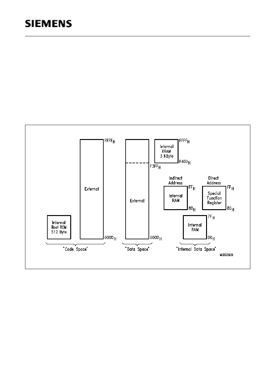
Memory Organization
The C509-L CPU manipulates data and operands in the following five address spaces:
≠ up to 64 Kbyte of external program memory
≠ up to 64 Kbyte of external data memory
≠ 512 byte of internal Boot ROM (program memory)
≠ 256 bytes of internal data memory
≠ 3 Kbyte of external XRAM data memory
≠ a 128 byte special function register area
Figure 5 illustrates the memory address spaces of the C509-L.
Figure 5
C509-L Memory Map
The C509-L can operate in four different operating modes (chipmodes) with different program and
data memory organizations :
≠ Normal Mode
≠ XRAM Mode
≠ Bootstrap Mode
≠ Programming Mode
Table 2 describes the program and data memory areas which are available in the different
chipmodes of the C509-L. It also shows the control bits of SFR SYSCON1, which are used for the
software selection of the chipmodes. Figures 6 to 9 shows the four chipmode configurations with
the code and data memory partitioning.
C509-L
Semiconductor Group
16
Table 2
Overview of Program and Data Memory Organization
Operating Mode
(Chipmode)
Program Memory
Data Memory
SYSCON1 Bits
Ext.
Int.
Ext.
Int.
PRGEN
1
SWAP
Normal Mode
0000H -
FFFFH
≠
0000H -
F3FFH
F400H
-
FFFFH
(XRAM)
0
0
XRAM Mode
0200H -
F3FFH
0000H -
01FFH =
Boot ROM;
F400H
-
FFFFH =
(XRAM)
0000H -
FFFFH
(read only)
≠
0
1
Bootstrap Mode
0200H -
F3FFH
0000H -
01FFH =
Boot ROM
0000H -
F3FFH
F400H
≠
FFFFH
(XRAM)
1
0
Programming Mode
0200H -
FFFFH
0000H -
01FFH =
Boot ROM;
F400H
-
FFFFH =
XRAM
0000H -
FFFFH
(read and
write)
≠
1
1
Semiconductor Group
17
09.96
C509-L
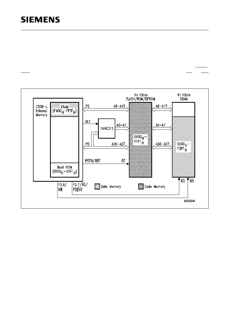
Normal Mode Configuration
The Normal Mode is the standard 8051 compatible operating mode of the C509-L. In this mode 64K
byte external code memory and 61K byte external SRAM as well as 3K byte internal data memory
(XRAM) are provided. If the is disabled (default after reset), totally 64K byte external data memory
are available. The Boot ROM is disabled. The external program memory is controlled by the PSEN/
RDF signal. Read and write accesses to the external data memory are controlled by the RD and WR
pins of port 3.
Figure 6
Locations of Code- and Data Memory in Normal Mode
C509-L
Semiconductor Group
18
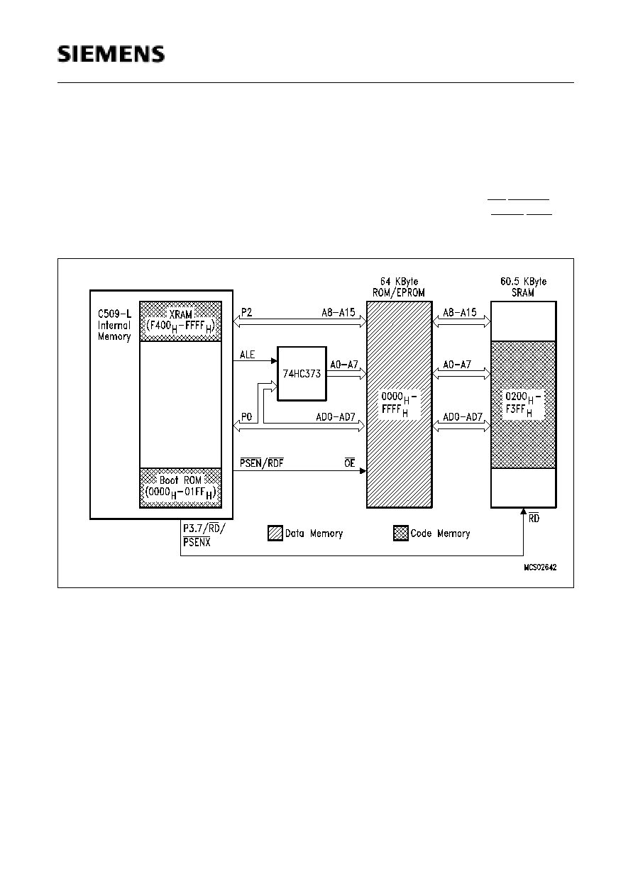
XRAM Mode Configuration
The XRAM Mode is implemented in the C509-L for executing e.g. up to 3K byte diagnostic software
which has been loaded into the XRAM in the Bootstrap Mode via the serial interface. In this
operating mode the Boot ROM, the XRAM, and the external data memory are mapped into the code
memory area, while the external ROM/EPROM is mapped into the external data memory area.
External program memory fetches from the SRAM are controlled by the P3.7/RD/PSENX pin.
External data memory read accesses from the ROM/EPROM are controlled by the PSEN/RDF pin.
In XRAM mode, the external data memory can only be read but not written.
Figure 7
Locations of Code- and Data Memory in XRAM Mode
Semiconductor Group
19
09.96
C509-L
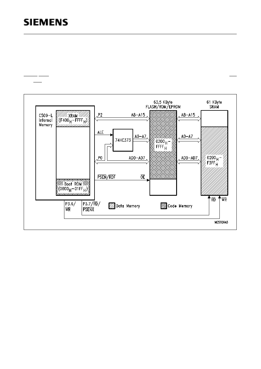
Bootstrap Mode Configuration
In the Bootstrap Mode the Boot ROM and the external FLASH/ROM/EPROM are mapped into the
code memory area. 61K byte external SRAM as well as 3K byte internal data memory (XRAM) are
provided in the external data memory area. The external program memory is controlled by the
PSEN/RDF signal. Read and write accesses to the external data memory are controlled by the RD
and WR pins of port 3.
Figure 8
Locations of Code- and Data Memory in Bootstrap Mode
C509-L
Semiconductor Group
20
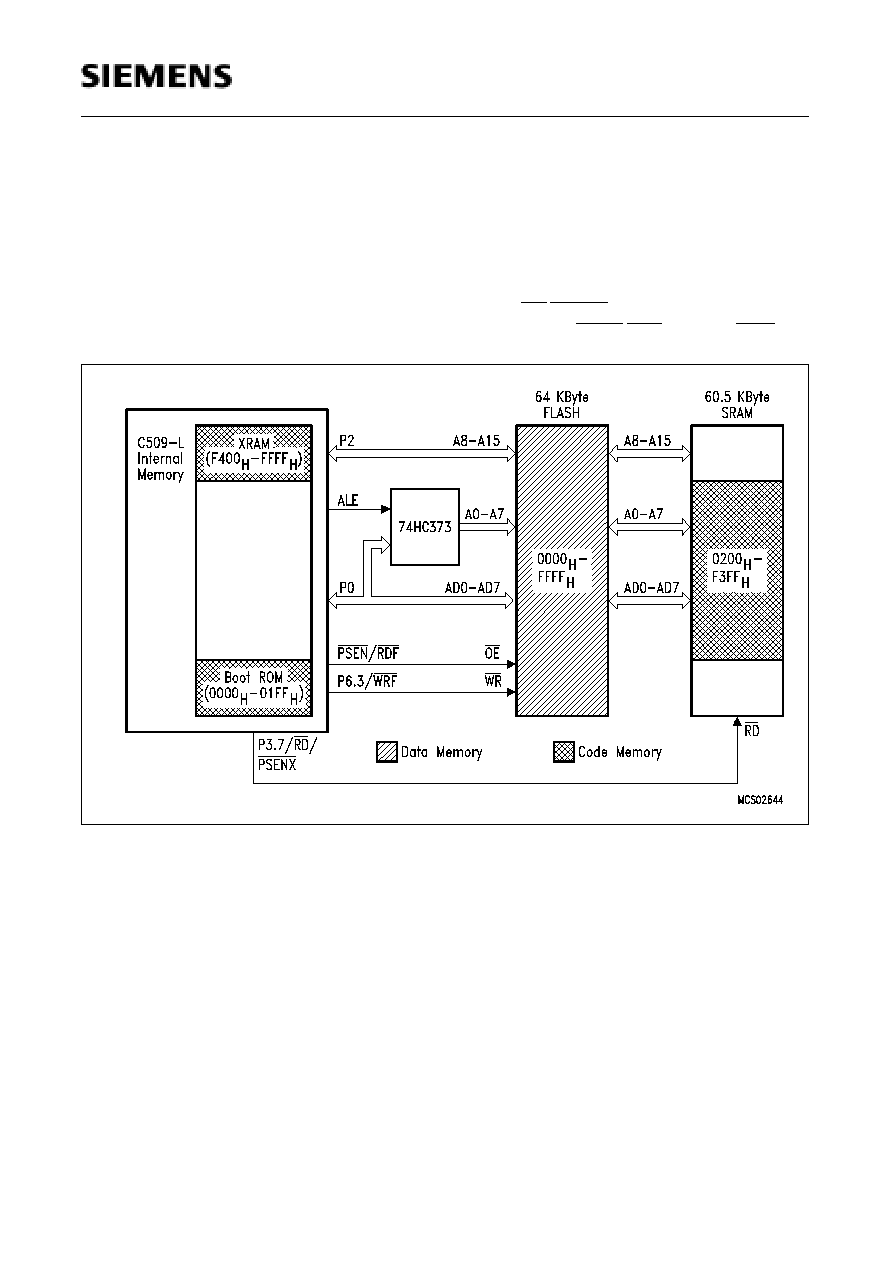
Programming Mode Configuration
The External Programming Mode is implemented for the in-circuit programming of external 5V-only
FLASH EPROMs. Similar as in the XRAM mode, the Boot ROM, the XRAM, and the external data
memory (SRAM) are mapped into the code memory area, while the external FLASH memory is
mapped into the external data memory area. Additionally to the XRAM mode, the FLASH memory
can also be written through external data memory accesses (MOVX instructions). External program
memory fetches from the SRAM are controlled by the P3.7/RD/PSENX pin. External data memory
read/write accesses from/to the ROM/EPROM are controlled by the PSEN/RDF and P6.3/WRF pin.
Figure 9
Locations of Code- and Data Memory in Programming Mode

Semiconductor Group
21
09.96
C509-L
The Bootstrap Loader
The C509-L includes a bootstrap mode, which is activated by setting the PRGEN pin at logic high
level at the rising edge of the RESET or the HWPD signal (bit PRGEN1=1). In this mode software
routines of the bootstrap loader, located at the addresses 0000H to 01FFH in the boot ROM will be
executed. Its purpose is to allow the easy and quick programming of the internal XRAM (F400H to
FFFFH) via serial interface while the MCU is in-circuit. This allows to transfer custom routines to the
XRAM, which will program an external 64 KByte FLASH memory. The serial routines of the
bootstrap loader may be replaced by own custom software or even can be blocked to prevent
unauthorized persons from reading out or writing to the external FLASH memory. Therefore the
bootstrap loader checks an external FLASH memory for existing custom software and executes it.
The bootstrap loader consists of three functional parts which represent the three phases as
described below.
Phase I : Check for existing custom software in the external FLASH memory and execute it.
Phase II : Establish a serial connection and automatically synchronize to the transfer speed (baud
rate) of the serial communication partner (host).
Phase III : Perform the serial communication to the host. The host controls the bootstrap loader by
sending header informations, which select one of four operating modes. These modes
are :
Mode 0 : Transfer a custom program from the host to the XRAM (F400H - FFFFH).
This mode returns to the beginning of phase III.
Mode 1 : Execute a custom program in the XRAM at any start address from F400H to
FFFFH.
Mode 2 : Check the contents of any area of the external FLASH memory by cal-
culating a checksum. This mode returns to the beginning of phase III.
Mode 3 : Execute a custom program in the FLASH memory at any start address
beyond 0200H (at addresses 0000H to 01FFH the boot-ROM is active).
The three phases of the bootstrap loader program and their connections are illustrated in figure 10.

C509-L
Semiconductor Group
22
Figure 10
The Three Phases of the Bootstrap Loader
The serial communication, which is activated in phase II is performed with the integrated serial
interface 0 of the C509-L. Using a full- or half-duplex serial cable (RS232) the MCU must be
connected to the serial port of the host computer as shown in figure .
Figure 11
Bootstrap Loader Interface to the PC
Semiconductor Group
23
09.96
C509-L
Control of XRAM Access
The XRAM in the C509-L is a memory area that is logically located at the upper end of the external
memory space, but is integrated on the chip. Because the XRAM is used in the same way as
external data memory the same instruction types (MOVX) must be used for accessing the XRAM.
Two bits in SFR SYSCON, XMAP0 and XMAP1, control the accesses to the XRAM.
Special Function Register SYSCON (Address B1H)
Reset Value : 1010XX01B
Bit XMAP0 is hardware protected. If it is reset once (XRAM access enabled) it cannot be set by
software. Only a reset operation will set the XMAP0 bit again.
The XRAM can be accessed by read/write instructions (MOVX A,DPTR, MOVX @DPTR,A), which
use the 16-bit DPTR for indirect addressing. For accessing the XRAM, the effective address stored
in DPTR must be in the range of F700H to FFFFH.38
The XRAM can be also accessed by read/write instructions (MOVX A,@Ri, MOVX @Ri,A), which
use only an 8-bit address (indirect addressing with registers R0 or R1). Therefore, a special page
register XPAGE which provides the upper address information (A8-A15) during 8-bit XRAM
accesses.
The behaviour of Port 0 and P2 during a MOVX access depends on the control bits XMAP0 and
XMAP1 in register SYSCON and on the state of pin EA. Table 3 lists the various operating
conditions.
Bit
Function
XMAP1
XRAM visible access control
Control bit for RD/WR signals during XRAMaccesses. If addresses are
outside the XRAM address range or if XRAM is disabled, this bit has no
effect.
XMAP1 = 0 : The signals RD and WR are not activated during accesses to
the XRAM
XMAP1 = 1 : Ports 0, 2 and the signals RD and WR are activated during
accesses to XRAM. In this mode, address and data
information during XRAM/CAN Controller accesses are
visible externally.
XMAP0
Global XRAM access enable/disable control
XMAP0 = 0 : The access to XRAM is enabled.
XMAP0 = 1 : The access to XRAM is disabled (default after reset!).
All MOVX accesses are performed via the external bus.
Further, this bit is hardware protected.
7
6
5
4
3
2
1
0
1
RMAP
≠
B1H
SYSCON
Bit No.
MSB
LSB
≠
XMAP1
CLKP
PMOD
XMAP0
The functions of the shaded bits are not used for XRAM control.

C509-L
Semiconductor Group
24
Table 3
Behaviour of P0/P2 and RD/WR During MOVX Accesses
EA = 0
EA = 1
XMAP1, XMAP0
XMAP1, XMAP0
00
10
X1
00
10
X1
MOVX
@DPTR
DPTR
<
XRAM
address
range
a)P0/P2
Bus
b)RD/WR active
c)ext.memory
is used
a)P0/P2
Bus
b)RD/WR active
c)ext.memory
is used
a)P0/P2
Bus
b)RD/WR active
c)ext.memory
is used
a)P0/P2
Bus
b)RD/WR active
c)ext.memory
is used
a)P0/P2
Bus
b)RD/WR active
c)ext.memory
is used
a)P0/P2
Bus
b)RD/WR active
c)ext.memory
is used
DPTR
XRAM
address
range
a)P0/P2
Bus
(WR / RD Data)
b)RD/WR
inactive
c)XRAM is used
a)P0/P2
Bus
(WR / RD Data)
b)RD/WR active
c)XRAM is used
a)P0/P2
Bus
b)RD/WR active
c) ext.memory
is used
a)P0/P2
I/0
b)RD/WR
inactive
c)XRAM is used
a)P0/P2
Bus
(WR / RD Data)
b)RD/WR active
c)XRAM is used
a)P0/P2
Bus
b)RD/WR active
c) ext.memory
is used
MOVX
@ Ri
XPAGE
<
XRAM
addr.page
range
a)P0
Bus
P2
I
/O
b)RD/WR active
c)ext.memory
is used
a)P0
Bus
P2
I
/O
b)RD/WR active
c)ext.memory
is used
a)P0
Bus
P2
I
/O
b)RD/WR active
c)ext.memory
is used
a)P0
Bus
P2
I
/O
b)RD/WR active
c)ext.memory
is used
a)P0
Bus
P2
I
/O
b)RD/WR active
c)ext.memory
is used
a)P0
Bus
P2
I
/O
b)RD/WR active
c)ext.memory
is used
XPAGE
XRAM
addr.page
range
a)P0
Bus
(WR / RD Data)
P2
I
/O
b)RD/WR
inactive
c)XRAM is used
a)P0
Bus
(WR / RD Data)
P2
I
/O
b)RD/WR active
c)XRAM is used
a)P0
Bus
P2
I
/O
b)RD/WR active
c)ext.memory
is used
a)P2
I
/O
P0/P2
I
/O
b)RD/WR
inactive
c)XRAM is used
a)P0
Bus
(WR / RD Data)
P2
I
/O
b)RD/WR active
c)XRAM is used
a)P0
Bus
P2
I
/O
b)RD/WR active
c)ext.memory
is used
modes compatible to 8051/C501 family
Semiconductor Group
25
09.96
C509-L
Reset and System Clock
The reset input is an active low input at pin RESET. Since the reset is synchronized internally, the
RESET pin must be held low for at least two machine cycles (12 oscillator periods) while the
oscillator is running. A pullup resistor is internally connected to
V
CC
to allow a power-up reset with
an external capacitor only. An automatic reset can be obtained when
V
CC
is applied by connecting
the reset pin to
V
SS
via a capacitor. Figure 12 shows the possible reset circuitries.
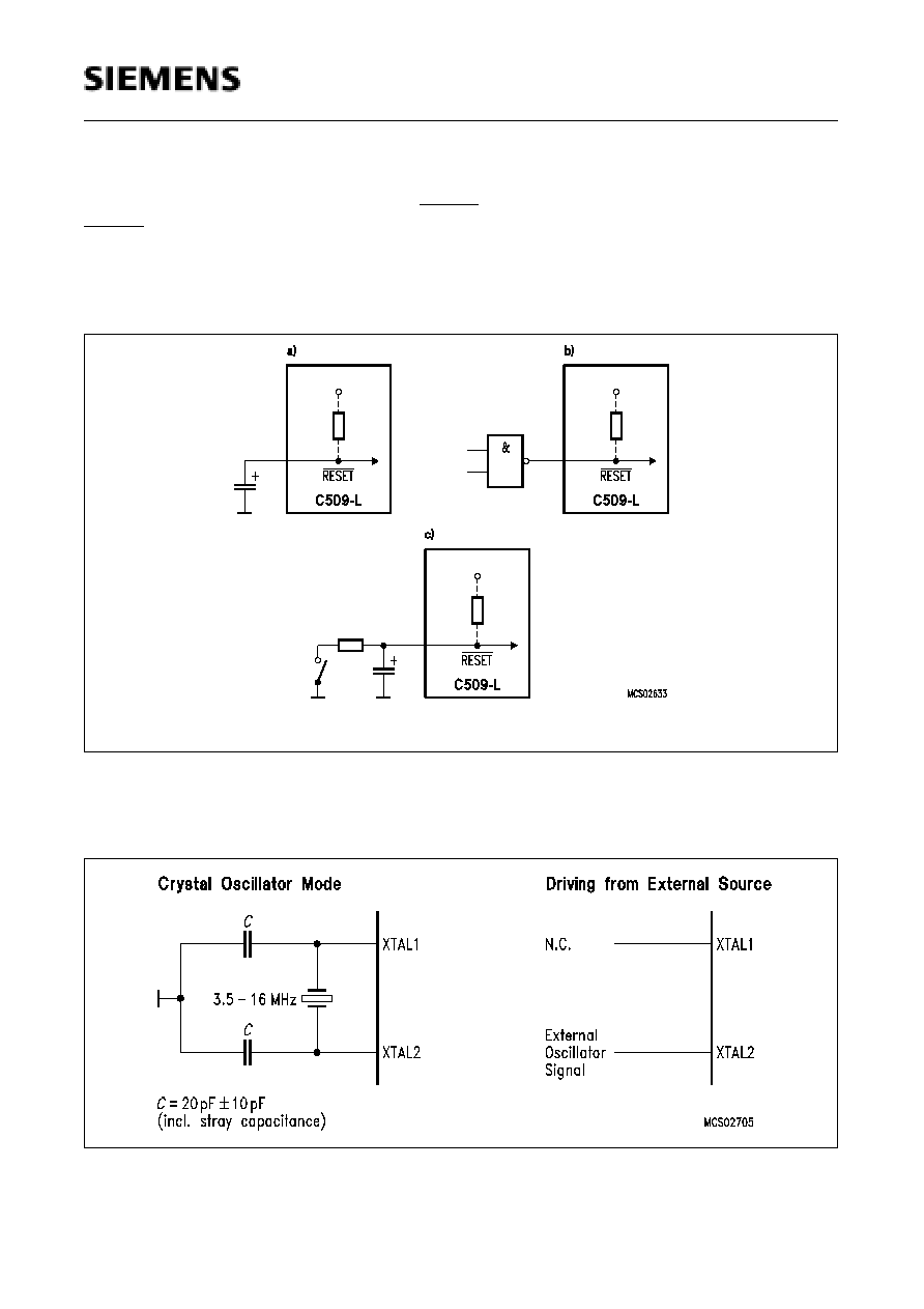
Figure 12
Reset Circuitries
Figure 13 shows the recommended oscillator circiutries for crystal and external clock operation.
Figure 13
Recommended Oscillator Circuitries
C509-L
Semiconductor Group
26
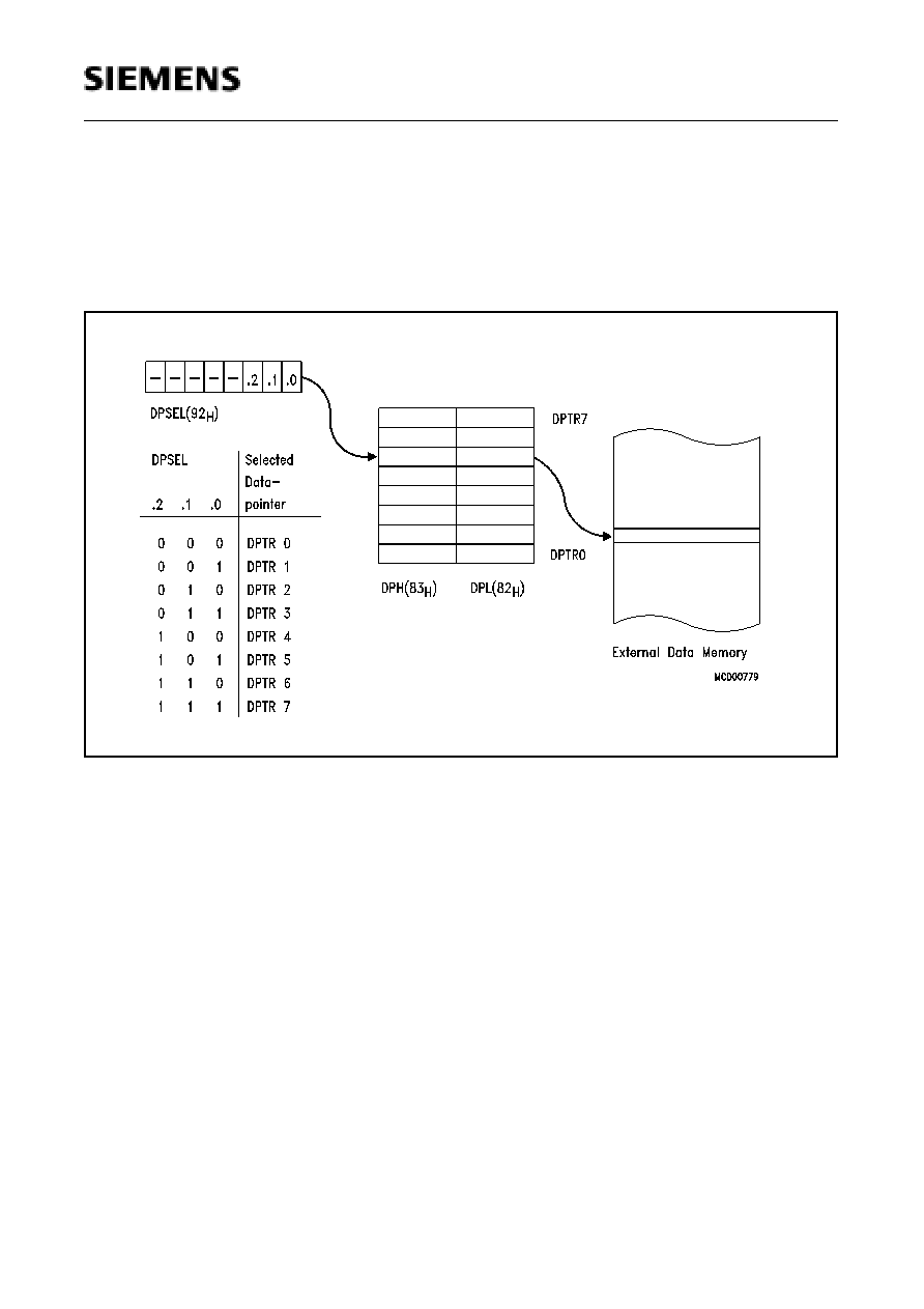
Multiple Datapointers
As a functional enhancement to the standard 8051 architecture, the C509-L contains eight 16-bit
datapointers instead of only one datapointer. The instruction set uses just one of these datapointers
at a time. The selection of the actual datapointer is done in the special function regsiter DPSEL.
Figure 14 illustrates the datapointer addressing mechanism.
Figure 14
External Data Memory Addressing using Multiple Datapointers
Semiconductor Group
27
09.96
C509-L
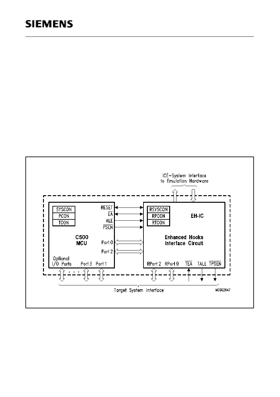
Enhanced Hooks Emulation Concept
The Enhanced Hooks Emulation Concept of the C500 microcontroller family is a new, innovative
way to control the execution of C500 MCUs and to gain extensive information on the internal
operation of the controllers. Emulation of on-chip ROM based programs is possible, too (not true for
the C509-L, because it lacks internal program memory).
Each production chip has built-in logic for the supprt of the Enhanced Hooks Emulation Concept.
Therefore, no costly bond-out chips are necessary for emulation. This also ensure that emulation
and production chips are identical.
The Enhanced Hooks Technology
TM
, which requires embedded logic in the C500 allows the C500
together with an EH-IC to function similar to a bond-out chip. This simplifies the design and reduces
costs of an ICE-system. ICE-systems using an EH-IC and a compatible C500 are able to emulate
all operating modes of the different versions of the C500 microcontrollers. This includes emulation
of ROM, ROM with code rollover and ROMless modes of operation. It is also able to operate in
single step mode and to read the SFRs after a break.
Figure 15
Basic C500 MCU Enhanced Hooks Concept Configuration
Port 0, port 2 and some of the control lines of the C500 based MCU are used by Enhanced Hooks
Emulation Concept to control the operation of the device during emulation and to transfer
informations about the programm execution and data transfer between the external emulation
hardware (ICE-system) and the C500 MCU.
C509-L
Semiconductor Group
28
Special Function Registers
All registers, except the program counter and the four general purpose register banks, reside in the
special function register area. Several special function registers of the C509-L (CC10-17, CT1REL,
CC1EN, CAFR) are located in the mapped special function register area. For accessing the mapped
special function register area, bit RMAP in special function register SYSCON must be set. All other
special function registers are located in the standard special function register area. As long as bit
RMAP is set, mapped special function registers can be accessed. This bit is not cleared by
hardware automatically.
Special Function Register SYSCON (Address B1H)
Reset Value : 1010XX01B
The 103 special function register (SFR) include pointers and registers that provide an interface
between the CPU and the other on-chip peripherals. The SFRs of the C509-L are listed in table 4
and table 5. In table 4 they are organized in groups which refer to the functional blocks of the C509-
L. Table 5 illustrates the contents of the SFRs in numeric order of their addresses. The most right
column of table 5 indicates if an SFR is accessed with a mapped procedure controlled by either
RMAP or PDIR.
Bit
Function
RMAP
Special function register map bit
RMAP = 0 : The access to the non-mapped (standard) special function
register area is enabled (reset value).
RMAP = 1 : The access to the mapped special function register area is
enabled.
7
6
5
4
3
2
1
0
1
RMAP
≠
B1H
SYSCON
Bit No.
MSB
LSB
≠
XMAP1
CLKP
PMOD
XMAP0
Semiconductor Group
29
09.96
C509-L
Table 4
Special Function Registers - Functional Blocks
Block
Symbol
Name
Address
Contents after
Reset
CPU
ACC
B
DPH
DPL
DPSEL
PSW
SP
SYSCON1
Accumulator
B-Register
Data Pointer, High Byte
Data Pointer, Low Byte
Data Pointer Select Register
Program Status Word
Stack Pointer
System Control Register 1
E0H
1
)
F0H
1
)
83H
82H
92H
D0H
1
)
81H
B2H
00H
00H
00H
00H
XXXXX000B
3)
00H
07H
00XXXEE0B
3)6)
SFR
Mapping
SYSCON
2)
System Control Register
B1H
1010XX01B
3)
Interrupt
System
IEN0
CTCON
2)
CT1CON
2)
IEN1
2)
IEN2
2)
IEN3
IP0
2)
IP1
2)
IRCON0
IRCON1
IRCON2
4)
EICC1
4)
TCON
2)
T2CON
2)
Interrupt Enable Register 0
Compare Timer Control Register
Compare Timer 1 Control Register
Interrupt Enable Register 1
Interrupt Enable Register 2
Interrupt Enable Register 3
Interrupt Priority Register 0
Interrupt Priority Register 1
Interrupt Request Control Register 0
Interrupt Request Control Register 1
Interrupt Request Control Register 2
Interrupt Request Enable Register for CT1
Timer Control Register
Timer 2 Control Register
A8H
1)
E1H
BCH
B8H
1)
9AH
BEH
A9H
B9H
C0H
1)
D1H
BFH
BFH
88H
1)
C8H
1)
00H
01000000B
3)
X1XX0000B
3)
00H
XX0000X0B
3)
XXXX00XXB
3)
00H
0X000000B
3)
00H
00H
00H
FFH
00H
00H
XRAM
XPAGE
SYSCON
2)
Page Address Register for XRAM
System Control Register
91H
B1H
00H
1010XX01B
3)
A/D
Converter
ADCON0
ADCON1
ADDATH
ADDATL
A/D Converter Control Register 0
A/D Converter Control Register 1
A/D Converter Data Register, High Byte
A/D Converter Data Register, Low Byte
D8H
1)
DCH
D9H
DAH
00H
01000000B
3
)
00H
00H
1)
Bit-addressable special function registers
2)
This special function register is listed repeatedly since some bits of it also belong to other functional blocks.
3)
X means that the value is indeterminate or the location is reserved
4)
Register is mapped by bit PDIR.
5)
Register is mapped by bit RMAP.
6)
"E" means that the value of the bit is defined by the logic level at pin PRGEN at the rising edge of the RESET
or HWPD signals
.
C509-L
Semiconductor Group
30
Compare /
Capture
Unit (CCU)
Timer 2
CCEN
CC4EN
CCH1
CCH2
CCH3
CCH4
CCL1
CCL2
CCL3
CCL4
CMEN
5)
CMH0
5)
CMH1
5)
CMH2
5)
CMH3
5)
CMH4
5)
CMH5
5)
CMH6
5)
CMH7
5)
CML0
5)
CML1
5)
CML2
5)
CML3
5)
CML4
5)
CML5
5)
CML6
5)
CML7
5)
CC1EN
5)
CC1H0
5)
CC1H1
5)
CC1H2
5)
CC1H3
5)
CC1H4
5)
CC1H5
5)
CC1H6
5)
CC1H7
5)
CC1L0
5)
CC1L1
5)
CC1L2
5)
CC1L3
5)
CC1L4
5)
CC1L5
5)
CC1L6
5)
CC1L7
5
CMSEL
5 )
Compare/Capture Enable Register
Compare/Capture 4 Enable Register
Compare/Capture Register 1, High Byte
Compare/Capture Register 2, High Byte
Compare/Capture Register 3, High Byte
Compare/Capture Register 4, High Byte
Compare/Capture Register 1, Low Byte
Compare/Capture Register 2, Low Byte
Compare/Capture Register 3, Low Byte
Compare/Capture Register 4, Low Byte
Compare Enable Register
Compare Register 0, High Byte
Compare Register 1, High Byte
Compare Register 2, High Byte
Compare Register 3, High Byte
Compare Register 4, High Byte
Compare Register 5, High Byte
Compare Register 6, High Byte
Compare Register 7, High Byte
Compare Register 0, Low Byte
Compare Register 1, Low Byte
Compare Register 2, Low Byte
Compare Register 3, Low Byte
Compare Register 4, Low Byte
Compare Register 5, Low Byte
Compare Register 6, Low Byte
Compare Register 7, Low Byte
Compare/Capture Enable Register
Compare/Capture 1 Register 0, High Byte
Compare/Capture 1 Register 1, High Byte
Compare/Capture 1 Register 2, High Byte
Compare/Capture 1 Register 3, High Byte
Compare/Capture 1 Register 4, High Byte
Compare/Capture 1 Register 5, High Byte
Compare/Capture 1 Register 6, High Byte
Compare/Capture 1 Register 7, High Byte
Compare/Capture 1 Register 0, Low Byte
Compare/Capture 1 Register 1, Low Byte
Compare/Capture 1 Register 2, Low Byte
Compare/Capture 1 Register 3, Low Byte
Compare/Capture 1 Register 4, Low Byte
Compare/Capture 1 Register 5, Low Byte
Compare/Capture 1 Register 6, Low Byte
Compare/Capture 1 Register 7, Low Byte
Compare Input Select
C1H
C9H
C3H
C5H
C7H
CFH
C2H
C4H
C6H
CEH
F6H
D3H
D5H
D7H
E3H
E5H
E7H
F3H
F5H
D2H
D4H
D6H
E2H
E4H
E6H
F2H
F4H
F6H
D3H
D5H
D7H
E3H
E5H
E7H
F3H
F5H
D2H
D4H
D6H
E2H
E4H
E6H
F2H
F4H
F7H
00H
00H
00H
00H
00H
00H
00H
00H
00H
00H
00H
00H
00H
00H
00H
00H
00H
00H
00H
00H
00H
00H
00H
00H
00H
00H
00H
00H
00H
00H
00H
00H
00H
00H
00H
00H
00H
00H
00H
00H
00H
00H
00H
00H
00H
5)
Register is mapped by bit RMAP.
Table 4
Special Function Registers - Functional Blocks (cont'd)
Block
Symbol
Name
Address
Contents after
Reset
Semiconductor Group
31
09.96
C509-L
Compare /
Capture
Unit (CCU)
Timer 2
cont'd
CAFR
5)
CRCH
CRCL
COMSETL
COMSETH
COMCLRL
COMCLRH
SETMSK
CLRMSK
CTCON
2)
CTRELH
5)
CTRELL
5)
CT1RELH
5)
CT1RELL
5)
TH2
TL2
T2CON
2)
CT1CON
2)
PRSC
2)
Capture 1, Falling/Rising Edge Register
Comp./Rel./Capt. Reg. High Byte
Comp./Rel./Capt. Reg. Low Byte
Compare Set Register, Low Byte
Compare Set Register, High Byte
Compare Clear Register, Low Byte
Compare Clear Register, High Byte
Compare Set Mask Register
Compare Clear Mask Register
Compare Timer Control Register
Compare Timer Rel. Reg., High Byte
Compare Timer Rel. Reg., Low Byte
Compare Timer 1 Rel. Reg., High Byte
Compare Timer 1 Rel. Reg., Low Byte
Timer 2, High Byte
Timer 2, Low Byte
Timer 2 Control Register
Compare Timer 1 Control Register
Prescaler Control Register
F7H
CBH
CAH
A1H
A2H
A3H
A4H
A5H
A6H
E1H
DFH
DEH
DFH
DEH
CDH
CCH
C8H
1)
BCH
B4H
00H
00H
00H
00H
00H
00H
00H
00H
00H
01000000B
3
)
00H
00H
00H
00H
00H
00H
00H
X1XX0000B
3)
11010101B
3)
Serial
Channels
ADCON0
2)
PCON
2)
S0BUF
S0CON
S0RELL
S0RELH
S1BUF
S1CON
S1RELL
S1RELH
A/D Converter Control Register
Power Control Register
Serial Channel 0 Buffer Register
Serial Channel 0 Control Register
Serial Channel 0 Reload Reg., Low Byte
Serial Channel 0 Reload Reg., High Byte
Serial Channel 1 Buffer Register
Serial Channel 1 Control Register
Serial Channel 1 Reload Reg., Low Byte
Serial Channel 1 Reload Reg., High Byte
D8H
1)
87H
99H
98H
1)
AAH
BAH
9CH
9BH
9DH
BBH
00H
00H
XXH
3
)
00H
D9H
XXXXXX11B
3)
XXH
3
)
01000000B
3)
00H
XXXXXX11B
3)
Watchdog
IEN0
2)
IEN1
2)
IP0
2)
IP1
2)
WDTREL
WDTL
6)
WDTH
6)
Interrupt Enable Register 0
Interrupt Enable Register 1
Interrupt Priority Register 0
Interrupt Priority Register 1
Watchdog Timer Reload Register
Watchdog Timer Register, Low Byte
Watchdog Timer Register, High Byte
A8H
1)
B8H
1)
A9H
B9H
86H
84H
85H
00H
00H
00H
0X000000B
3
)
00H
00H
00H
1)
Bit-addressable special function registers
2)
This special function register is listed repeatedly since some bits of it also belong to other functional blocks.
3)
X means that the value is indeterminate or the location is reserved
4)
Register is mapped by bit PDIR.
5)
Register is mapped by bit RMAP.
6)
Registers are only readable and cannot be written.
Table 4
Special Function Registers - Functional Blocks (cont'd)
Block
Symbol
Name
Address
Contents after
Reset

C509-L
Semiconductor Group
32
MUL/DIV
Unit
ARCON
MD0
MD1
MD2
MD3
MD4
MD5
Arithmetic Control Register
Multiplication/Division Register 0
Multiplication/Division Register 1
Multiplication/Division Register 2
Multiplication/Division Register 3
Multiplication/Division Register 4
Multiplication/Division Register 5
EFH
E9H
EAH
EBH
ECH
EDH
EEH
0XXXXXXXB
3)
XXH
3)
XXH
3)
XXH
3)
XXH
3)
XXH
3)
XXH
3)
Timer 0 /
Timer 1
TCON
TH0
TH1
TL0
TL1
TMOD
PRSC
2)
Timer Control Register
Timer 0, High Byte
Timer 1, High Byte
Timer 0, Low Byte
Timer 1, Low Byte
Timer Mode Register
Prescaler Control Register
88H
1)
8CH
8DH
8AH
8BH
89H
B4H
00H
00H
00H
00H
00H
00H
11010101B
3)
Ports
P0
4)
DIR0
4)
P1
4)
DIR1
4)
P2
4)
DIR2
4)
P3
4)
DIR3
4)
P4
4)
DIR4
4)
P5
4)
DIR5
4)
P6
4)
DIR6
4)
P7
P8
P9
4)
DIR9
4)
Port 0
Direction Register Port 0
Port 1
Direction Register Port 1
Port 2
Direction Register Port 2
Port 3
Direction Register Port 3
Port 4
Direction Register Port 4
Port 5
Direction Register Port 5
Port 6
Direction Register Port 6
Port 7, Analog/Digital Input
Port 8, Analog/Digital Input
Port 9
Direction Register Port 9
80H
1)
80H
1)
90H
1)
90H
1)
A0H
1)
A0H
1)
B0H
1)
B0H
1)
E8H
1)
E8H
1)
F8H
1)
F8H
1)
FAH
FAH
DBH
DDH
F9H
F9H
FFH
FFH
FFH
FFH
FFH
FFH
FFH
FFH
FFH
FFH
FFH
FFH
FFH
FFH
--
--
FFH
FFH
Power
Saving
Modes
PCON
Power Control Register
87H
00H
1)
Bit-addressable special function registers
2)
This special function register is listed repeatedly since some bits of it also belong to other functional blocks.
3)
X means that the value is indeterminate and the location is reserved
4)
Register is mapped by bit PDIR.
5)
Register is mapped by bit RMAP.
Table 4
Special Function Registers - Functional Blocks (cont'd)
Block
Symbol
Name
Address
Contents after
Reset
Semiconductor Group
33
09.96
C509-L
Table 5
Contents of the SFRs, SFRs in numeric order of their addresses
Addr
Register
Content
after
Reset
1)
Bit 7
Bit 6
Bit 5
Bit 4
Bit 3
Bit 2
Bit 1
Bit 0
Mapped
by
2)
80
H
P0
FF
H
.7
.6
.5
.4
.3
.2
.1
.0
PDIR=
0
80
H
DIR0
FF
H
.7
.6
.5
.4
.3
.2
.1
.0
PDIR=1
81
H
SP
07
H
.7
.6
.5
.4
.3
.2
.1
.0
≠
82
H
DPL
00
H
.7
.6
.5
.4
.3
.2
.1
.0
≠
83
H
DPH
00
H
.7
.6
.5
.4
.3
.2
.1
.0
≠
84
H
WDTL
00
H
.7
.6
.5
.4
.3
.2
.1
.0
≠
85
H
WDTH
00
H
.7
.6
.5
.4
.3
.2
.1
.0
≠
86
H
WDTREL
00
H
WPSEL
.6
.5
.4
.3
.2
.1
.0
≠
87
H
PCON
00
H
SMOD
PDS
IDLS
SD
GF1
GF0
PDE
IDLE
≠
88
H
TCON
00
H
TF1
TR1
TF0
TR0
IE1
IT1
IE0
IT0
≠
89
H
TMOD
00
H
GATE
C/T
M1
M0
GATE
C/T
M1
M0
≠
8A
H
TL0
00
H
.7
.6
.5
.4
.3
.2
.1
.0
≠
8B
H
TL1
00
H
.7
.6
.5
.4
.3
.2
.1
.0
≠
8C
H
TH0
00
H
.7
.6
.5
.4
.3
.2
.1
.0
≠
8D
H
TH1
00
H
.7
.6
.5
.4
.3
.2
.1
.0
≠
90
H
P1
FF
H
T2
CLK-
OUT
T2EX
INT2
INT6
INT5
INT4
INT3
PDIR=
0
90
H
DIR1
FF
H
.7
.6
.5
.4
.3
.2
.1
.0
PDIR=1
91
H
XPAGE
00
H
.7
.6
.5
.4
.3
.2
.1
.0
≠
92
H
DPSEL
XXXX.
X000
B
≠
≠
≠
≠
≠
.2
.1
.0
≠
98
H
S0CON
00
H
SM0
SM1
SM20
REN0
TB80
RB80
TI0
RI0
≠
99
H
S0BUF
XX
H
.7
.6
.5
.4
.3
.2
.1
.0
≠
9A
H
IEN2
XX00.
00X0
B
≠
≠
ECR
ECS
ECT
ECMP
≠
ES1
≠
9B
H
S1CON
0100.
0000
B
SM
S1P
SM21
REN1
TB81
RB81
TI1
RI1
≠
9C
H
S1BUF
XX
H
.7
.6
.5
.4
.3
.2
.1
.0
≠
9D
H
S1RELL
00
H
.7
.6
.5
.4
.3
.2
.1
.0
≠
A0
H
P2
FF
H
.7
.6
.5
.4
.3
.2
.1
.0
PDIR=0
A0
H
DIR2
FF
H
.7
.6
.5
.4
.3
.2
.1
.0
PDIR=1
A1
H
COMSETL 00
H
.7
.6
.5
.4
.3
.2
.1
.0
≠
1) X means that the value is indeterminate or the location is reserved.
2) SFRs with a comment in this column are mapped registers.
Shaded registers are bit-addressable special function registers.
C509-L
Semiconductor Group
34
A2
H
COMSETH 00
H
.7
.6
.5
.4
.3
.2
.1
.0
≠
A3
H
COMCLRL 00
H
.7
.6
.5
.4
.3
.2
.1
.0
≠
A4
H
COMCLRH 00
H
.7
.6
.5
.4
.3
.2
.1
.0
≠
A5
H
SETMSK
00
H
.7
.6
.5
.4
.3
.2
.1
.0
≠
A6
H
CLRMSK
00
H
.7
.6
.5
.4
.3
.2
.1
.0
≠
A8
H
IEN0
00
H
EAL
WDT
ET2
ES0
ET1
EX1
ET0
EX0
≠
A9
H
IP0
00
H
OWDS WDTS
.5
.4
.3
.2
.1
.0
≠
AA
H
S0RELL
D9
H
.7
.6
.5
.4
.3
.2
.1
.0
≠
B0
H
P3
FF
H
RD
WR
T1
T0
INT1
INT0
TxD0
RxD0
PDIR=0
B0
H
DIR3
FF
H
.7
.6
.5
.4
.3
.2
.1
.0
PDIR=1
B1
H
SYSCON
1010.
XX01
B
CLKP
PMOD
1
RMAP
≠
≠
XMAP1 XMAP0 ≠
B2
H
SYSCON1
3)
00XX.
XEE0
B
ESWC
SWC
≠
EA1
EA0
PRGEN1 PRGEN0
SWAP
≠
B4
H
PRSC
1101.
0101
B
WDTP
S0P
T2P1
T2P0
T1P1
T1P0
T0P1
T0P0
≠
B8
H
IEN1
00
H
EXEN2 SWDT
EX6
EX5
EX4
EX3
EX2
EADC
≠
B9
H
IP1
0X00.
0000
B
PDIR
≠
.5
.4
.3
.2
.1
.0
≠
BA
H
S0RELH
XXXX.
XX11
B
≠
≠
≠
≠
≠
≠
.1
.0
≠
BB
H
S1RELH
XXXX.
XX11
B
≠
≠
≠
≠
≠
≠
.1
.0
≠
BC
H
CT1CON
X1XX.
0000
B
≠
CT1P
≠
≠
CT1F
CLK12
CLK11
CLK10
≠
BE
H
IEN3
XXXX.
00XX
B
≠
≠
≠
≠
ECT1
ECC1
≠
≠
≠
BF
H
IRCON2
00
H
ICC17
ICC16
ICC15
ICC14
ICC13
ICC12
ICC11
ICC10
PDIR=0
BF
H
EICC1
FF
H
EICC17
EICC16
EICC15
EICC14
EICC13
EICC12
EICC11
EICC10
PDIR=1
C0
H
IRCON0
00
H
EXF2
TF2
IEX6
IEX5
IEX4
IEX3
IEX2
IADC
≠
C1
H
CCEN
00
H
COCAH3 COCAL3 COCAH2 COCAL2 COCAH1 COCAL1 COCAH0 COCAL0
≠
1) X means that the value is indeterminate or the location is reserved.
2) SFRs with a comment in this column are mapped registers.
3) "E" means that the value of the bit is defined by the logic level at pin PRGEN at the rising edge of the RESET
or HWPD signals
.
Shaded registers are bit-addressable special function registers.
Table 5
Contents of the SFRs, SFRs in numeric order of their addresses (cont'd)
Addr
Register
Content
after
Reset
1)
Bit 7
Bit 6
Bit 5
Bit 4
Bit 3
Bit 2
Bit 1
Bit 0
Mapped
by
2)

Semiconductor Group
35
09.96
C509-L
C2
H
CCL1
00
H
.7
.6
.5
.4
.3
.2
.1
.0
≠
C3
H
CCH1
00
H
.7
.6
.5
.4
.3
.2
.1
.0
≠
C4
H
CCL2
00
H
.7
.6
.5
.4
.3
.2
.1
.0
≠
C5
H
CCH2
00
H
.7
.6
.5
.4
.3
.2
.1
.0
≠
C6
H
CCL3
00
H
.7
.6
.5
.4
.3
.2
.1
.0
≠
C7
H
CCH3
00
H
.7
.6
.5
.4
.3
.2
.1
.0
≠
C8
H
T2CON
00
H
T2PS
I3FR
I2FR
T2R1
T2R0
T2CM
T2I1
T2I0
≠
C9
H
CC4EN
00
H
COCO
EN1
COCO
N2
COCO
N1
COCO
N0
COCO
EN0
COCAH
4
COCAL
4
COM0
≠
CA
H
CRCL
00
H
.7
.6
.5
.4
.3
.2
.1
.0
≠
CB
H
CRCH
00
H
.7
.6
.5
.4
.3
.2
.1
.0
≠
CC
H
TL2
00
H
.7
.6
.5
.4
.3
.2
.1
.0
≠
CD
H
TH2
00
H
.7
.6
.5
.4
.3
.2
.1
.0
≠
CE
H
CCL4
00
H
.7
.6
.5
.4
.3
.2
.1
.0
≠
CF
H
CCH4
00
H
.7
.6
.5
.4
.3
.2
.1
.0
≠
D0
H
PSW
00
H
CY
AC
F0
RS1
RS0
OV
F1
P
≠
D1
H
IRCON1
00
H
ICMP7
ICMP6
ICMP5
ICMP4
ICMP3
ICMP2
ICMP1
ICMP0
≠
D2
H
CML0
00
H
.7
.6
.5
.4
.3
.2
.1
.0
RMAP=0
D2
H
CC1L0
00
H
.7
.6
.5
.4
.3
.2
.1
.0
RMAP=1
D3
H
CMH0
00
H
.7
.6
.5
.4
.3
.2
.1
.0
RMAP=0
D3
H
CC1H0
00
H
.7
.6
.5
.4
.3
.2
.1
.0
RMAP=1
D4
H
CML1
00
H
.7
.6
.5
.4
.3
.2
.1
.0
RMAP=0
D4
H
CC1L1
00
H
.7
.6
.5
.4
.3
.2
.1
.0
RMAP=1
D5
H
CMH1
00
H
.7
.6
.5
.4
.3
.2
.1
.0
RMAP=0
D5
H
CC1H1
00
H
.7
.6
.5
.4
.3
.2
.1
.0
RMAP=1
D6
H
CML2
00
H
.7
.6
.5
.4
.3
.2
.1
.0
RMAP=0
D6
H
CC1L2
00
H
.7
.6
.5
.4
.3
.2
.1
.0
RMAP=1
D7
H
CMH2
00
H
.7
.6
.5
.4
.3
.2
.1
.0
RMAP=0
D7
H
CC1H2
00
H
.7
.6
.5
.4
.3
.2
.1
.0
RMAP=1
D8
H
ADCON0
00
H
BD
CLK
ADEX
BSY
ADM
MX2
MX1
MX0
≠
D9
H
ADDATH
00
H
.7
(MSB)
.6
.5
.4
.3
.2
.1
.0
≠
1) X means that the value is indeterminate or the location is reserved.
2) SFRs with a comment in this column are mapped registers.
Shaded registers are bit-addressable special function registers.
Table 5
Contents of the SFRs, SFRs in numeric order of their addresses (cont'd)
Addr
Register
Content
after
Reset
1)
Bit 7
Bit 6
Bit 5
Bit 4
Bit 3
Bit 2
Bit 1
Bit 0
Mapped
by
2)
C509-L
Semiconductor Group
36
DA
H
ADDATL
00
H
.7
.6
(LSB)
≠
≠
≠
≠
≠
≠
≠
DB
H
P7
≠
.7
.6
.5
.4
.3
.2
.1
.0
≠
DC
H
ADCON1
0100.
0000
B
ADCL1 ADCL0 ADST1 ADST0 MX3
MX2
MX1
MX0
≠
DD
H
P8
≠
≠
.6
.5
.4
.3
.2
.1
.0
≠
DE
H
CTRELL
00
H
.7
.6
.5
.4
.3
.2
.1
.0
RMAP=0
DE
H
CT1RELL
00
H
.7
.6
.5
.4
.3
.2
.1
.0
RMAP=1
DF
H
CTRELH
00
H
.7
.6
.5
.4
.3
.2
.1
.0
RMAP=0
DF
H
CT1RELH
00
H
.7
.6
.5
.4
.3
.2
.1
.0
RMAP=1
E0
H
ACC
00
H
.7
.6
.5
.4
.3
.2
.1
.0
≠
E1
H
CTCON
0100.
0000
B
T2PS1
CTP
ICR
ICS
CTF
CLK2
CLK1
CLK0
≠
E2
H
CML3
00
H
.7
.6
.5
.4
.3
.2
.1
.0
RMAP=0
E2
H
CC1L3
00
H
.7
.6
.5
.4
.3
.2
.1
.0
RMAP=1
E3
H
CMH3
00
H
.7
.6
.5
.4
.3
.2
.1
.0
RMAP=0
E3
H
CC1H3
00
H
.7
.6
.5
.4
.3
.2
.1
.0
RMAP=1
E4
H
CML4
00
H
.7
.6
.5
.4
.3
.2
.1
.0
RMAP=0
E4
H
CC1L4
00
H
.7
.6
.5
.4
.3
.2
.1
.0
RMAP=1
E5
H
CMH4
00
H
.7
.6
.5
.4
.3
.2
.1
.0
RMAP=0
E5
H
CC1H4
00
H
.7
.6
.5
.4
.3
.2
.1
.0
RMAP=1
E6
H
CML5
00
H
.7
.6
.5
.4
.3
.2
.1
.0
RMAP=0
E6
H
CC1L5
00
H
.7
.6
.5
.4
.3
.2
.1
.0
RMAP=1
E7
H
CMH5
00
H
.7
.6
.5
.4
.3
.2
.1
.0
RMAP=0
E7
H
CC1H5
00
H
.7
.6
.5
.4
.3
.2
.1
.0
RMAP=1
E8
H
P4
FF
H
CM7
CM6
CM5
CM4
CM3
CM2
CM1
CM0
PDIR=0
E8
H
DIR4
FF
H
.7
.6
.5
.4
.3
.2
.1
.0
PDIR=1
E9
H
MD0
XX
H
.7
.6
.5
.4
.3
.2
.1
.0
≠
EA
H
MD1
XX
H
.7
.6
.5
.4
.3
.2
.1
.0
≠
EB
H
MD2
XX
H
.7
.6
.5
.4
.3
.2
.1
.0
≠
EC
H
MD3
XX
H
.7
.6
.5
.4
.3
.2
.1
.0
≠
ED
H
MD4
XX
H
.7
.6
.5
.4
.3
.2
.1
.0
≠
1) X means that the value is indeterminate or the location is reserved.
2) SFRs with a comment in this column are mapped registers.
Shaded registers are bit-addressable special function registers.
Table 5
Contents of the SFRs, SFRs in numeric order of their addresses (cont'd)
Addr
Register
Content
after
Reset
1)
Bit 7
Bit 6
Bit 5
Bit 4
Bit 3
Bit 2
Bit 1
Bit 0
Mapped
by
2)
Semiconductor Group
37
09.96
C509-L
EE
H
MD5
XX
H
.7
.6
.5
.4
.3
.2
.1
.0
≠
EF
H
ARCON
0XXX.
XXXX
B
MDEF
MDOV
SLR
SC.4
SC.3
SC.2
SC.1
SC.0
≠
F0
H
B
00
H
.7
.6
.5
.4
.3
.2
.1
.0
≠
F2
H
CML6
00
H
.7
.6
.5
.4
.3
.2
.1
.0
RMAP=0
F2
H
CC1L6
00
H
.7
.6
.5
.4
.3
.2
.1
.0
RMAP=1
F3
H
CMH6
00
H
.7
.6
.5
.4
.3
.2
.1
.0
RMAP=0
F3
H
CC1H6
00
H
.7
.6
.5
.4
.3
.2
.1
.0
RMAP=1
F4
H
CML7
00
H
.7
.6
.5
.4
.3
.2
.1
.0
RMAP=0
F4
H
CC1L7
00
H
.7
.6
.5
.4
.3
.2
.1
.0
RMAP=1
F5
H
CMH7
00
H
.7
.6
.5
.4
.3
.2
.1
.0
RMAP=0
F5
H
CC1H7
00
H
.7
.6
.5
.4
.3
.2
.1
.0
RMAP=1
F6
H
CMEN
00
H
.7
.6
.5
.4
.3
.2
.1
.0
RMAP=0
F6
H
CC1EN
00
H
.7
.6
.5
.4
.3
.2
.1
.0
RMAP=1
F7
H
CMSEL
00
H
.7
.6
.5
.4
.3
.2
.1
.0
RMAP=0
F7
H
CAFR
00
H
.7
.6
.5
.4
.3
.2
.1
.0
RMAP=1
F8
H
P5
FF
H
CCM7
CCM6
CCM5
CCM4
CCM3
CCM2
CCM1
CCM0
PDIR=0
F8
H
DIR5
FF
H
.7
.6
.5
.4
.3
.2
.1
.0
PDIR=1
F9
H
P9
FF
H
CC17
CC16
CC15
CC14
CC13
CC12
CC11
CC10
PDIR=0
F9
H
DIR9
FF
H
.7
.6
.5
.4
.3
.2
.1
.0
PDIR=1
FA
H
P6
FF
H
.7
.6.
.5
.4
.3
TxD1
RxD1
ADST
PDIR=0
FA
H
DIR6
FF
H
.7
.6
.5
.4
.3
.2
.1
.0
PDIR=1
1) X means that the value is indeterminate or the location is reserved.
2) SFRs with a comment in this column are mapped registers.
Shaded registers are bit-addressable special function registers.
Table 5
Contents of the SFRs, SFRs in numeric order of their addresses (cont'd)
Addr
Register
Content
after
Reset
1)
Bit 7
Bit 6
Bit 5
Bit 4
Bit 3
Bit 2
Bit 1
Bit 0
Mapped
by
2)

C509-L
Semiconductor Group
38
Digital I/O Ports
The C509-L allows for digital I/O on 64 lines grouped into 8 bidirectional 8-bit ports. Each port bit
consists of a latch, an output driver and an input buffer. Read and write accesses to the I/O ports P0
through P6 and P9 are performed via their corresponding special function registers P0 to P6 and
P9. The port structure of the C509-L is designed to operate either as a quasi-bidirectional port
structure, compatible to the standard 8051-Family, or as a genuine bidirectional port structure. This
port operating mode can be selected by software (setting or clearing the bit PMOD in the SFR
SYSCON).
The output drivers of port 0 and 2 and the input buffers of port 0 are also used for accessing external
memory. In this application, port 0 outputs the low byte of the external memory address, time-
multiplexed with the byte being written or read. Port 2 outputs the high byte of the external memory
address when the address is 16 bits wide. Otherwise, the port 2 pins continue emitting the P2 SFR
contents.
Analog Input Ports
Ports 7 and 8 are available as input ports only and provide for two functions. When used as digital
inputs, the corresponding SFR's P7 and P8 contain the digital value applied to port 7 and port 8
lines. When used for analog inputs the desired analog channel is selected by a three-bit field in SFR
ADCON0 or a four-bit field in SFR ADCON1. Of course, it makes no sense to output a value to these
input-only ports by writing to the SFR's P7 or P8; this will have no effect.
lf a digital value is to be read, the voltage levels are to be held within the input voltage specifications
(
V
IL
/
V
IH
). Since P7 and P8 are not bit-addressable registers, all input lines of P7 or P8 are read at the
same time by byte instructions.
Nevertheless, it is possible to use ports 7 and 8 simultaneously for analog and digital input.
However, care must be taken that all bits of P7 or P8 that have an undetermined value caused by
their analog function are masked.
Semiconductor Group
39
09.96
C509-L
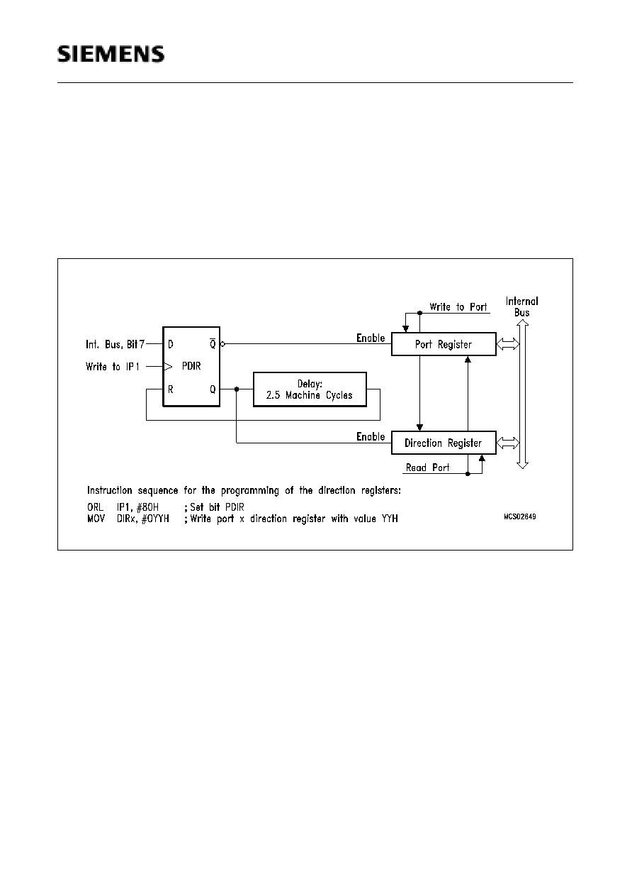
Port Structure Selection
After a reset operation of the C509-L, the quasi-bidirectional 8051-compatible port structure is
selected. For selection of the bidirectional port structure (CMOS) the bit PMOD of SFR SYSCON
must be set. Because each port pin can be programmed as an input or an output, additionally, after
the selection of the bidirectional mode the direction register of the ports must be written (except the
analog/digital input ports 7,8). This direction registers are mapped to the port registers. This means,
the port register address is equal to its direction register address. Figure 16 illustrates the port- and
direction register configuration.
Figure 16
Port Register, Direction Register
For the access the direction registers a double instruction sequence must be executed. The first
instruction has to set bit PDIR in SFR IP1. Thereafter, a second instruction can read or write the
direction registers. PDIR will automatically be cleared after the second machine cycle (S2P2) after
having been set. For this time, the access to the direction register is enabled and the register can
be read or written. Further, the double instruction sequence as shown in figure 16, cannot be
interrupted by an interrupt,
When the bidirectional port structure is activated (bit PMOD in SFR SYSCON =1) after a reset, the
ports are defined as inputs (direction registers default values after reset are set to FFH).
With PMOD = 0 (quasi-bidirectional port structure selected), any access to the direction registers
has no effect on the port driver circuitries.
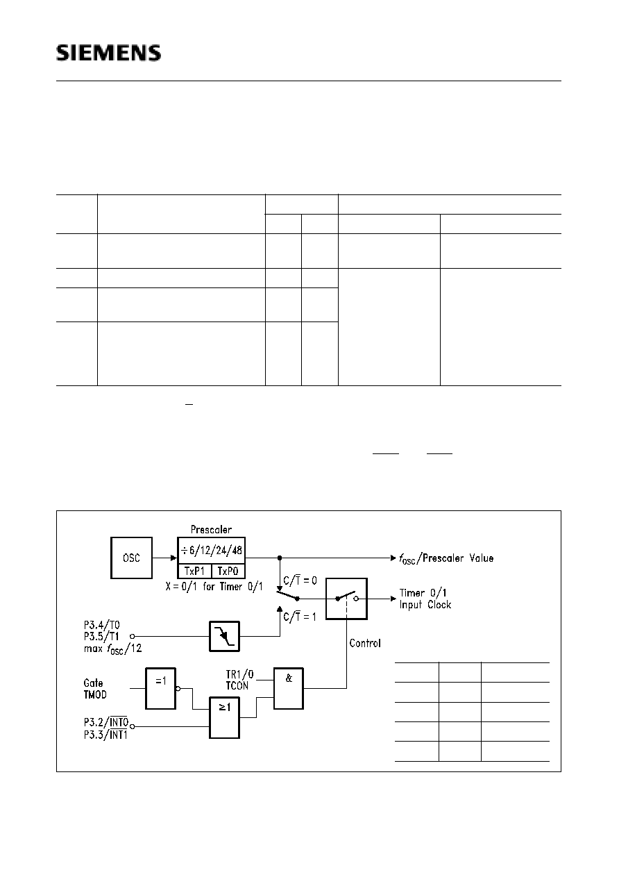
C509-L
Semiconductor Group
40
Timer / Counter 0 and 1
Timer/Counter 0 and 1 can be used in four operating modes as listed in table 6 :
In the "timer" function (C/T = `0') the register is incremented by a count rate of
f
OSC
/6 up to
f
OSC
/32.
In the "counter" function the register is incremented in response to a 1-to-0 transition at its
corresponding external input pin (P3.4/T0, P3.5/T1). Since it takes two machine cycles to detect a
falling edge the max. count rate is
f
OSC
/12. External inputs INT0 and INT1 (P3.2, P3.3) can be
programmed to function as a gate to facilitate pulse width measurements. Figure 17 illustrates the
input clock logic of timer 0/1.
Figure 17
Timer/Counter 0 and 1 Input Clock Logic
Table 6
Timer/Counter 0 and 1 Operating Modes
Mode
Description
TMOD
Input Clock
M1
M0
internal
external (max)
0
8-bit timer/counter with a
divide-by-32 prescaler
0
0
f
OSC
/6x32 up to
f
OSC
/48x32
f
OSC
/12x32
1
16-bit timer/counter
0
1
f
OSC
/6 up to
f
OSC
/
48
f
OSC
/12
2
8-bit timer/counter with
8-bit autoreload
1
0
3
Timer/counter 0 used as one
8-bit timer/counter and one
8-bit timer
Timer 1 stops
1
1
TxP1
TxP0
Prescaler
0
0
6
0
1
12
1
0
24
1
1
48
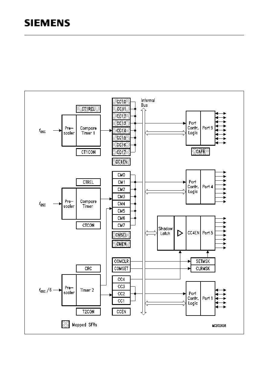
Semiconductor Group
41
09.96
C509-L
Compare / Capture Unit (CCU)
The compare/capture unit can be used in all kinds of digital signal generation and event capturing
like pulse generation, pulse width modulation, pulse width measuring etc. The CCU consists of
three 16-bit timer/counters and an array of several compare or compare/capture registers. A set of
control registers is used for flexible adapting of the CCU to a wide variety of applications.
Figure 18
Block Diagram of the CCU

C509-L
Semiconductor Group
42
The block diagram in figure 18 shows the general configuration of the CCU. All CC1 to CC4
registers and the CRC register are exclusively assigned to timer 2. Each of the eight compare
registers CM0 through CM7 can either be assigned to timer 2 or to the faster compare timer, e.g. to
provide up to 8 PWM output channels. The assignment of the CMx registers - which can be done
individually for every single register - is combined with an automatic selection of one of the two
possible compare modes. The compare/capture registers CC10 to CC17 and the reload register
CT1REL are assigned to compare timer 1 and are mapped to the corresponding registers of the
compare timer.
The compare function and the reaction of the corresponding outputs depend on the timer/compare
register combination. Table 7 shows the possible configurations of the CCU and the corresponding
compare modes which can be selected. The following sections describe the function of these
configurations.
Table 7
CCU Configurations
Assigned
Timer
Compare
Register
Compare Output at
Possible Modes
Timer 2
CRCH/CRCL
CCH1/CCL1
CCH2/CCL2
CCH3/CCL3
CCH4/CCL4
P1.0/INT3/CC0
P1.1/INT4/CC1
P1.2/INT5/CC2
P1.3/INT6/CC3
P1.4/INT2/CC4
Compare mode 0, 1 + Reload
Compare mode 0, 1 / capture
Compare mode 0, 1 / capture
Compare mode 0, 1 / capture
Compare mode 0, 1 / capture)
CCH4/CCL4
P1.4/INT2/CC4
P5.0/CCM0
to
P5.7/CCM7
Compare mode 1
"Concurrent compare"
CMH0/CML0
to
CMH7/CML7
P4.0/CM0
to
P4.7/CM7
Compare mode 0
COMSET
COMCLR
P5.0/CCM0
to
P5.7/CCM7
Compare mode 2
Compare
Timer
CMH0/CML0
to
CMH7/CML7
P4.0/CM0
to
P4.7/CM7
Compare mode 1
Compare
Timer 1
CC1H0/CC1L0
to
CC1H7/CC1L7
P5.0/CCM0
to
P5.7/CCM7
Compare mode 0 / capture
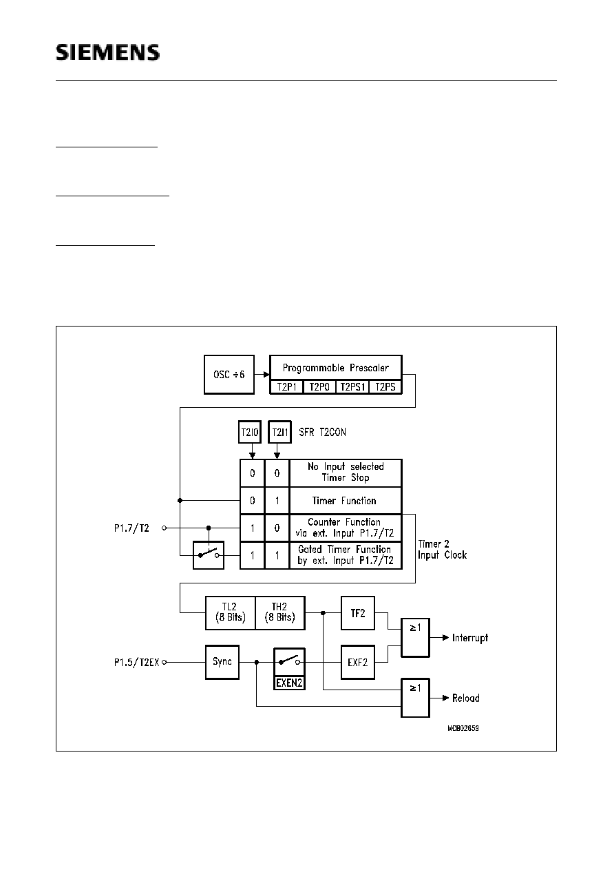
Semiconductor Group
43
09.96
C509-L
Timer 2 Operation
Gated Timer Mode : In gated timer function, the external input pin P1.7/T2 operates as a gate to the
input of timer 2. lf T2 is high, the internal clock input is gated to the timer. T2 = 0 stops the counting
procedure.The external gate signal is sampled once every machine cycle.
Event Counter Mode : In the event counter function, the timer 2 is incremented in response to a 1-
to-0 transition at its corresponding external input pin P1.7/T2. In this function, the external input is
sampled every machine cycle. The maximum count rate is 1/12 of the oscillator frequency.
Reload of Timer 2 : Two reload modes are selectable:
In mode 0, when timer 2 rolls over from all 1's to all 0's, it not only sets TF2 but also causes the timer
2 registers to be loaded with the 16-bit value in the CRC register, which is preset by software.
In mode 1, a 16-bit reload from the CRC register is caused by a negative transition at the correspon-
ding input pin P1.5/T2EX.
Figure 19
Block Diagram of Timer 2
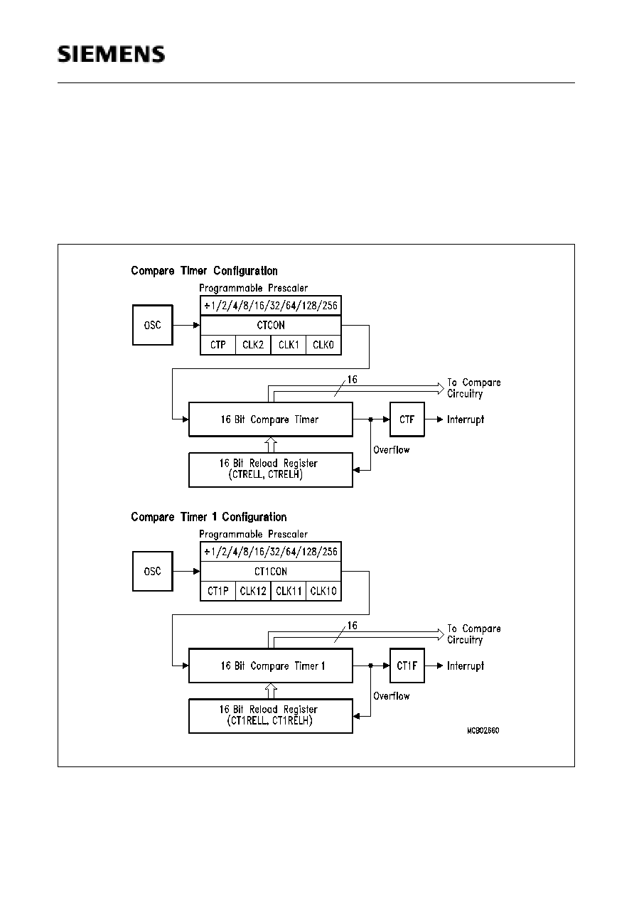
C509-L
Semiconductor Group
44
Compare Timer Operation
The compare timers receive its input clock from a programmable prescaler which provides input
frequencies, ranging from
f
OSC
up to
f
OSC
/256. The compare timers are, once started, free-running
16-bit timers, which on overflow are automatically reloaded by the contents of the 16-bit reload
registers. The compare timers have - as any other timer in the C509-L - their own interrupt request
flags CTF and CT1F. These flags are set when the timer count rolls over from all ones to the reload
value. Figure 20 shows the block diagram of compare timer and compare timer 1.
Figure 20
Compare Timer and Compare Timer 1 Block Diagram

Semiconductor Group
45
09.96
C509-L
Compare Modes
The compare function of a timer/register combination operates as follows. the 16-bit value stored in
a compare or compare/capture register is compared with the contents of the timer register. lf the
count value in the timer register matches the stored value, an appropriate output signal is generated
at a corresponding port pin. Several timer/compare register combinations are selectable (see table
7). In these configurations three cdifferent ompare modes are selectable.
Compare Mode 0
In compare mode 0, upon matching the timer and compare register contents, the output signal
changes from low to high. lt goes back to a low level on timer overflow. As long as compare mode
0 is enabled, the appropriate output pin is controlled by the timer circuit only and writing to the port
will have no effect. Figure 21 shows a functional diagram of a port circuit when used in compare
mode 0. The port latch is directly controlled by the timer overflow and compare match signals. The
input line from the internal bus and the write-to-latch line of the port latch are disconnected when
compare mode 0 is enabled.
Figure 21
Port Latch in Compare Mode 0
Compare Mode 1
Ilf compare mode 1 is enabled (can only be selected for compare registers assigned to timer 2) and
the software writes to the appropriate output latch at the port, the new value will not appear at the
output pin until the next compare match occurs. Thus, it can be choosen whether the output signal
has to make a new transition (1-to-0 or 0-to-1, depending on the actual pin-level) or should keep its
old value at the time when the timer value matches the stored compare value.
In compare mode 1 (see figure 22) the port circuit consists of two separate latches. One latch
(which acts as a "shadow latch") can be written under software control, but its value will only be
transferred to the port latch (and thus to the port pin) when a compare match occurs.
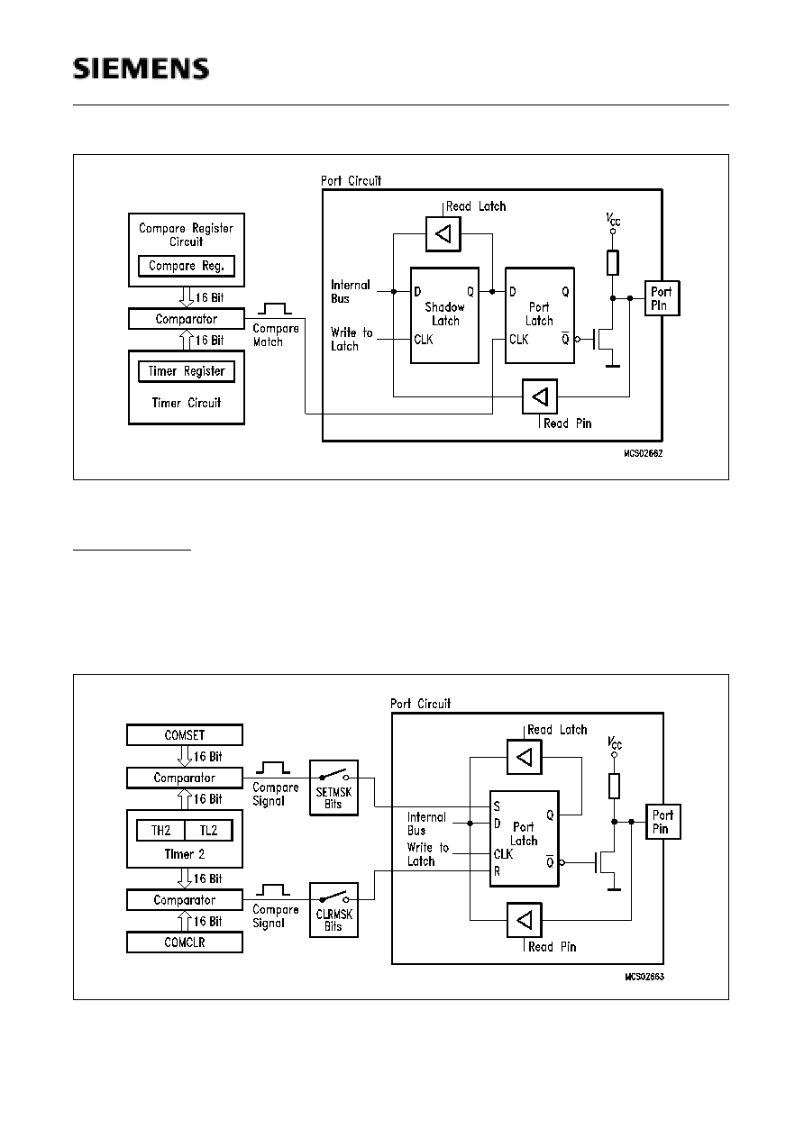
C509-L
Semiconductor Group
46
Figure 22
Compare Function in Compare Mode 1
Compare Mode 2
In the compare mode 2 the port 5 pins are under control of compare/capture register CC4, but under
control of the compare registers COMSET and COMCLR. When a compare match occurs with
register COMSET, a high level appears at the pins of port 5 when the corresponding bits in the mask
register SETMSK are set. When a compare match occurs with register COMCLR, a low level
appears at the pins of port 5 when the corresponding bits in the mask register CLRMSK are set.
Figure 23
Compare Function of Compare Mode 2

Semiconductor Group
47
09.96
C509-L
Multiplication / Division Unit (MDU)
This on-chip arithmetic unit of the C509-L provides fast 32-bit division, 16-bit multiplication as well
as shift and normalize features. All operations are unsigned integer operations. Table 8 describes
the five general operations the MDU is able to perform.
1) 1
t
CY
= 6
∑
CLP = 1 machine cycle = 375 ns at 16-MHz oscillator frequency
2) The maximal shift speed is 6 shifts per machine cycle
The MDU consists of seven special function registers (MD0-MD5, ARCON) which are used as
operand, result, and control registers. The three operation phases are shown in figure 24.
Figure 24
Operating Phases of the MDU
Table 8
MDU Operation Characteristics
Operation
Result
Remainder
Execution Time
32bit/16bit
16bit/16bit
16bit x 16bit
32-bit normalize
32-bit shift L/R
32bit
16bit
32bit
≠
≠
16bit
16bit
≠
≠
≠
6
t
CY
1)
4
t
CY
1)
4
t
CY
1)
6
t
CY
2)
6
t
CY
2)
C509-L
Semiconductor Group
48
For starting an operation, registers MD0 to MD5 and ARCON must be written to in a certain
sequence according table 8 and 9. The order the registers are accessed determines the type of the
operation. A shift operation is started by a final write operation to SFR ARCON.
Abbrevations :
D'end
: Dividend, 1st operand of division
D'or
: Divisor, 2nd operand of division
M'and
: Multiplicand, 1st operand of multiplication
M'or
: Multiplicator, 2nd operand of multiplication
Pr
: Product, result of multiplication
Rem
: Remainder
Quo
: Quotient, result of division
...L
: means, that this byte is the least significant of the 16-bit or 32-bit operand
...H
: means, that this byte is the most significant of the 16-bit or 32-bit operand
Table 9
Programming the MDU for Multiplication and Division
Operation
32Bit/16Bit
16Bit/16Bit
16Bit x 16Bit
First Write
Last Write
MD0
D'endL
MD1
D'end
MD2
D'end
MD3
D'endH
MD4
D'orL
MD5
D'orH
MD0
D'endL
MD1
D'endH
MD4
D'orL
MD5
D'orH
MD0
M'andL
MD4
M'orL
MD1
M'andH
MD5
M'orH
First Read
Last Read
MD0
QuoL
MD1
Quo
MD2
Quo
MD3
QuoH
MD4
RemL
MD5
RemH
MD0
QuoL
MD1
QuoH
MD4
RemL
MD5
RemH
MD0
PrL
MD1
MD2
MD3
PrH
Table 10
Programming athe MDU for a Shift or Normalize Operation
Operation
Normalize, Shift Left, Shift Right
First write
Last write
MD0
least significant byte
MD1
.
MD2
.
MD3
most significant byte
ARCON
start of conversion
First read
Last read
MD0
least significant byte
MD1
.
MD2
.
MD3
most significant byte
Semiconductor Group
49
09.96
C509-L
Serial Interfaces 0 and 1
The C509-L has two serial interfaces which are functionally nearly identical concerning the
asynchronous modes of operation. The two channels are full-duplex, meaning they can transmit
and receive simultaneously. The serial channel 0 is completely compatible with the serial channel
of the C501 (one synchronous mode, three asynchronous modes). Serial channel 1 has the same
functionality in its asynchronous modes, but the synchronous mode and the fixed baud rate UART
mode is missing.
The operating modes of the serial interfaces is illustrated in table 11. The possible baudrates can
be calculated using the formulas given in table 12.
Table 11
Operating Modes of Serial Interface 0 and 1
Serial
Interface
Mode
S0CON
S1CON
Description
SM0
SM1
SM
0
0
0
0
≠
Shift register mode
Serial data enters and exits through R
◊
D0;
T
◊
D0 outputs the shift clock; 8-bit are
transmitted/received (LSB first); fixed baud rate
1
0
1
≠
8-bit UART, variable baud rate
10 bits are transmitted (through T
◊
D0) or
received (at R
◊
D0)
2
1
0
≠
9-bit UART, fixed baud rate
11 bits are transmitted (through T
◊
D0) or
received (at R
◊
D0)
3
1
1
≠
9-bit UART, variable baud rate
Like mode 2
1
A
≠
≠
0
9-bit UART; variable baud rate
11 bits are transmitted (through T
◊
D1) or
received (at R
◊
D1)
B
≠
≠
1
8-bit UART; variable baud rate
10 bits are transmitted (through T
◊
D1) or
received (at R
◊
D1)
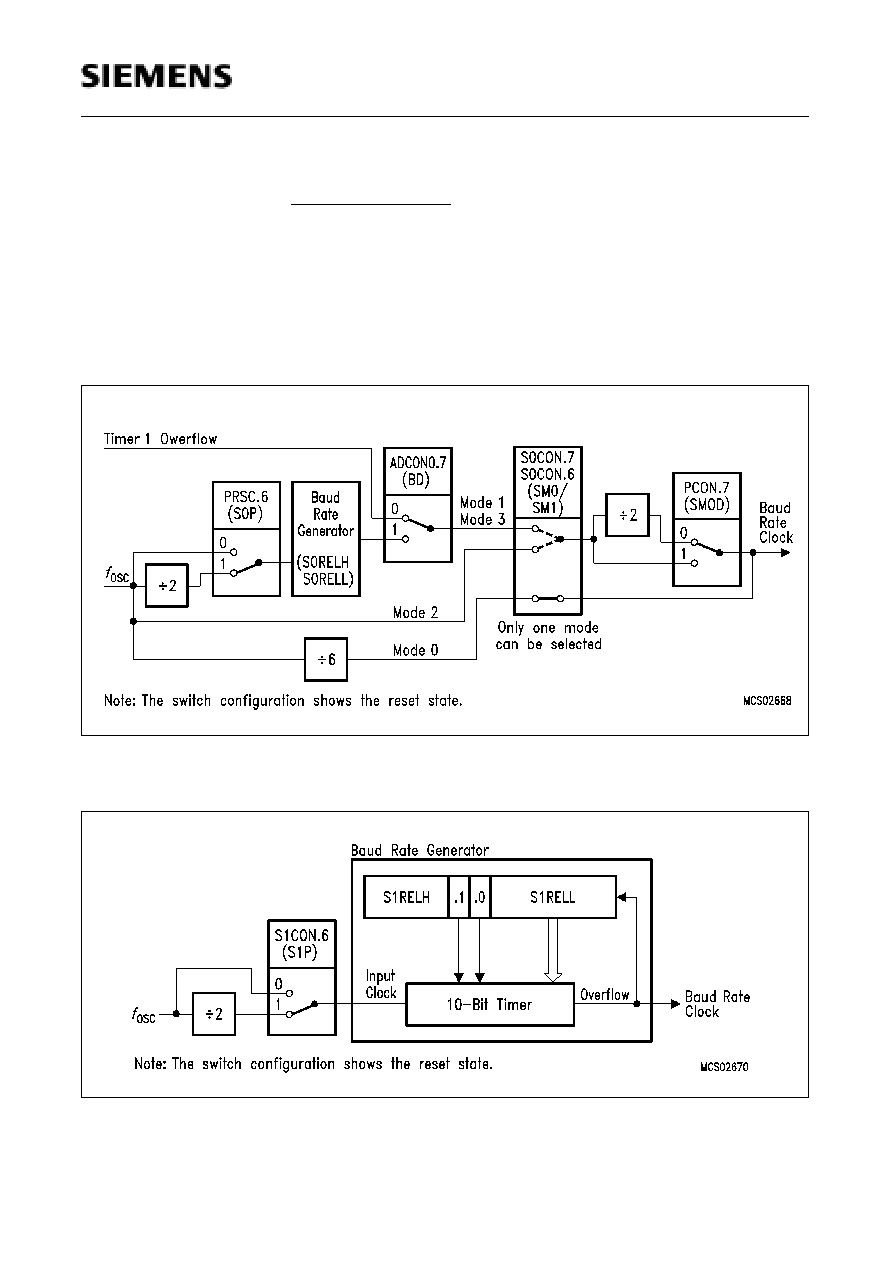
C509-L
Semiconductor Group
50
For clarification some terms regarding the difference between "baud rate clock" and "baud rate"
should be mentioned. In the asynchronous modes the serial interfaces require a clock rate which is
16 times the baud rate for internal synchronization. Therefore, the baud rate generators/timers have
to provide a "baud rate clock" (output signal in figure 25 and figure 26) to the serial interface
which - there divided by 16 - results in the actual "baud rate". Further, the abrevation f
OSC
refers to
the oscillator frequency (crystal or external clock operation).
The variable baud rates for modes 1 and 3 of the serial interface 0 can be derived from either timer
1 or a decdicated baud rate generator (see figure 25). The variable baud rates for modes A and B
of the serial interface 1 are derived from a decdicated baud rate generator as shown in figure 26.
Figure 25
Serial Interface 0 : Baud Rate Generation Configuration
Figure 26
Serial Interface 1 : Baud Rate Generator Configuration
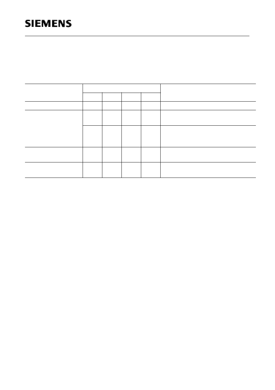
Semiconductor Group
51
09.96
C509-L
Table 12 below lists the values/formulas for the baud rate calculation of serial interface 0 and 1 with
its dependencies of the control bits BD, SMOD, S0P, and S1P.
Table 12
Serial Interface 0 - Baud Rate Dependencies
Serial Interface 0
Operating Modes
Active Control Bits
Baud Rate Calculation
BD
S0P
SMOD S1P
Mode 0 (Shift Register)
≠
≠
≠
≠
f
OSC
/ 6
Mode 1 (8-bit UART)
Mode 3 (9-bit UART)
0
≠
0 or 1
≠
Controlled by timer 1 overflow :
(2
SMOD
◊
timer 1 overflow rate) / 32
1
0 or 1
0 or 1
≠
Controlled by baud rate generator :
(2
S0P
◊
2
SMOD
◊
f
OSC
) /
(64
◊
baud rate generator overflow rate)
Mode 2 (9-bit UART)
≠
≠
0
1
≠
f
OSC
/ 32
f
OSC
/ 16
Mode A (9-bit UART)
Mode B (8-bit UART)
≠
≠
≠
0 or 1
(2
S1P
◊
f
OSC
) /
(32
◊
baud rate generator overflow rate)

C509-L
Semiconductor Group
52
10-Bit A/D Converter
The C509-L has a high perfomance 10-bit A/D converter (figure 27) with 15 inputs included which
uses successive approximation technique for the conversion and uses self calibration mechanisms
for reduction and compensation of offset and linearity errors
Figure 27
A/D Converter Block Diagram

Semiconductor Group
53
09.96
C509-L
The A/D converter provides the following features:
≠ 15 multiplexed input channels, which can also be used as digital inputs (port 7, port 8)
≠ 10-bit resolution
≠ Single or continuous conversion mode
≠ Internal or external start-of-conversion trigger capability
≠ Programmable conversion and sample clock
≠ Interrupt request generation after each conversion
≠ Using successive approximation conversion technique via a capacitor array
≠ Built-in hidden calibration of offset and linearity errors
The A/D converter uses basically three clock signals for operation : the input clock f
IN
(=1/t
IN
), the
conversion clock f
ADC
(=1/t
ADC
) and the sample clock f
SC
(=1/t
SC
). All clock signals are derived
from the C509-L system clock f
OSC
which is applied at the XTAL pins. The input clock f
IN
is equal
to f
OSC
while the conversion clock and the sample clock must be adapted. The conversion clock is
limited to a maximum frequency of 2 MHz. The table in figure 28 defines the divider ratio for the
conversion and sample clock of each combination of the prescaler bits.
Figure 28
A/D Converter Clock Selection
Conversion Clock
f
ADC
Sample Clock
f
SC
ADCL1 ADCL0
f
ADC
ADST1 ADST0
0
0
ADST1 ADST0
0
1
ADST1 ADST0
1
0
ADST1 ADST0
1
1
0
0
f
IN
/ 4
f
IN
/ 8
f
IN
/ 16
f
IN
/ 32
f
IN
/ 64
0
1
f
IN
/ 8
f
IN
/ 16
f
IN
/ 32
f
IN
/ 64
f
IN
/ 128
1
0
f
IN
/ 16
f
IN
/ 32
f
IN
/ 64
f
IN
/ 128
f
IN
/ 256
1
1
f
IN
/ 32
f
IN
/ 64
f
IN
/ 128
f
IN
/ 256
f
IN
/ 512

C509-L
Semiconductor Group
54
A/D Conversion Timing
An A/D conversion is internally started by writing into the SFR ADDATL with dummy data. A write
to SFR ADDATL will start a new conversion even if a conversion is currently in progress. Basically,
the A/D conversion procedure is divided into three parts :
≠ Sample phase (t
S
), used for sampling the analog input voltage.
≠ Conversion phase (t
CO
), used for the real A/D conversion.(includes calibration)
≠ Write result phase (t
WR
), used for writing the conversion result into the ADDAT registers.
The total A/D conversion time is defined by t
ADCC
which is the sum of the two phase times t
S
and
t
CO
. The duration of the two phases of an A/D conversion is specified by its specific timing
parameter as shown in figure 29.
Figure 29
A/D Conversion Timing
Conversion Clock
Prescaler
ADCL1 ADCL0
Sample Clock
Prescaler
ADST1 ADST0
Sample
Time
t
S
Conversion
Time
t
CO
ConversionTime
t
ADCC
Number of
CPU Cycles
0
0
0
0
0
1
1
0
1
1
8 x t
IN
16 x t
IN
32 x t
IN
64 x t
IN
40 x t
IN
48 x t
IN
56 x t
IN
72 x t
IN
104 x t
IN
8
9
12
17
0
1
0
0
0
1
1
0
1
1
16 x t
IN
32 x t
IN
64 x t
IN
128 x t
IN
80 x t
IN
96 x t
IN
112 x t
IN
144 x t
IN
208 x t
IN
16
18
24
34
1
0
0
0
0
1
1
0
1
1
32 x t
IN
64 x t
IN
128 x t
IN
256 x t
IN
160 x t
IN
192 x t
IN
224 x t
IN
288 x t
IN
416 x t
IN
32
37
48
69
1
1
0
0
0
1
1
0
1
1
64 x t
IN
128 x t
IN
256 x t
IN
512 x t
IN
320 x t
IN
384 x t
IN
448 x t
IN
576 x t
IN
832 x t
IN
64
74
96
138
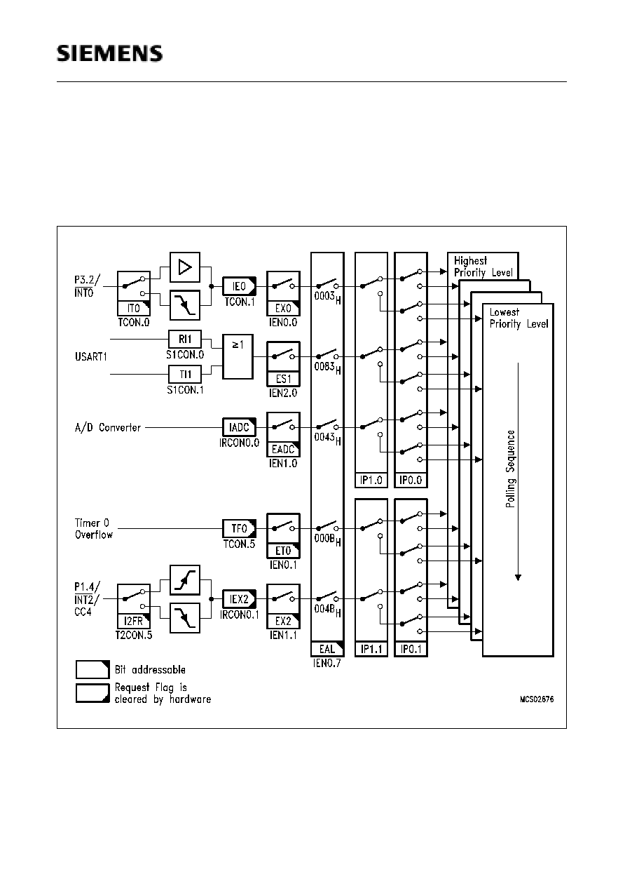
Semiconductor Group
55
09.96
C509-L
Interrupt System
The C509-L provides 19 interrupt sources with four priority levels. 12 interrupts can be generated by
the on-chip peripherals and 7 interrupts may be triggered externally. In the C509-L the 19 interrupt
sources are combined to six groups of three or four interrupt sources. Each interrupt group can be
programmed to one of the four interrupt priority levels. Figure 30 to 33 give a general overview of
the interrupt sources and illustrate the interrupt request and control flags.
Figure 30
Interrupt Request Sources (Part 1)
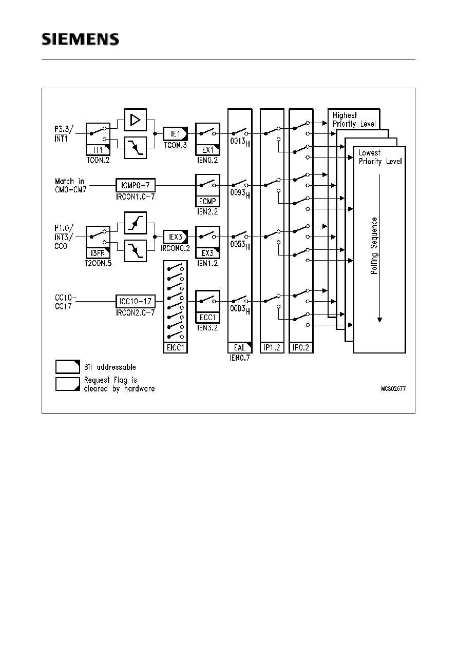
C509-L
Semiconductor Group
56
Figure 31
Interrupt Request Sources (Part 2)
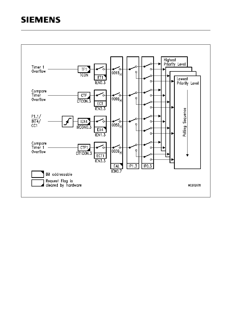
Semiconductor Group
57
09.96
C509-L
Figure 32
Interrupt Request Sources (Part 3)
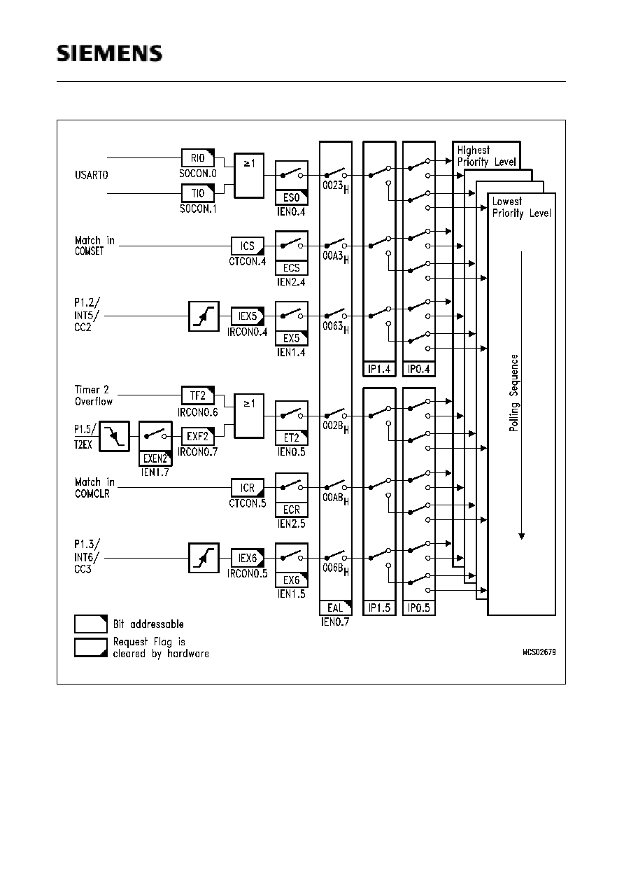
C509-L
Semiconductor Group
58
Figure 33
Interrupt Request Sources (Part 4)
Semiconductor Group
59
09.96
C509-L
Table 13
Interrupt Sources and their Corresponding Interrupt Vectors
Interrupt Source
Interrupt Vector Address
Interrupt Request Flags
External Interrupt 0
0003H
IE0
Timer 0 Overflow
000BH
TF0
External Interrupt 1
0013H
IE1
Timer 1 Overflow
001BH
TF1
Serial Channel 0
0023H
RI0 / TI0
Timer 2 Overflow / Ext. Reload
002BH
TF2 / EXF2
A/D Converter
0043H
IADC
External Interrupt 2
004BH
IEX2
External Interrupt 3
0053H
IEX3
External Interrupt 4
005BH
IEX4
External Interrupt 5
0063H
IEX5
External Interrupt 6
006BH
IEX6
Serial Channel 1
0083H
RI1 / TI1
Compare Match Interupt of
Compare Registers CM0-CM7
assigned to Timer 2
0093H
ICMP0 - ICMP7
Compare Timer Overflow
009BH
CTF
Compare Match Interupt of
Compare Register COMSET
00A3H
ICS
Compare Match Interupt of
Compare Register COMCLR
00ABH
ICR
Compare / Capture Event interrupt 00D3H
ICC10 - ICC17
Compare Timer 1 Overflow
00DBH
CT1F
C509-L
Semiconductor Group
60
Fail Save Mechanisms
The C509-L offers two on-chip peripherals which monitor the program flow and ensure an automatic
"fail-safe" reaction for cases where the controller's hardware fails or the software hangs up:
≠ A programmable watchdog timer (WDT) with variable time-out period from 189 microseconds
up to approx. 0.79 seconds at 16 MHz.
≠ An oscillator watchdog (OWD) which monitors the on-chip oscillator and forces the
microcontroller into the reset state if the on-chip oscillator fails.
Programmable Watchdog Timer
The watchdog timer in the C509-L is a 15-bit timer, which is incremented by a count rate of
f
OSC
/12
up to
f
OSC
/384. For programming of the watchdog timer overflow rate, the upper 7 bit of the watchdog
timer can be written. Figure 34 shows the block diagram of the watchdog timer unit.
Figure 34
Block Diagram of the Programmable Watchdog Timer
The watchdog timer can be started by software (bit SWDT) or by hardware through pin PE/SWD,
but it cannot be stopped during active mode of the C509-L. If the software fails to refresh the running
watchdog timer an internal reset will be initiated on watchdog timer overflow. For refreshing of the
watchdog timer the content of the SFR WDTREL is transferred to the upper 7-bit of the watchdog
timer. The refresh sequence consists of two consecutive instructions which set the bits WDT and
SWDT each. The reset cause (external reset or reset caused by the watchdog) can be examined
by software (flag WDTS). It must be noted, however, that the watchdog timer is halted during the
idle mode and power down mode of the processor.
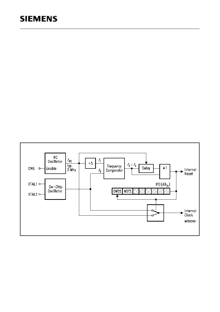
Semiconductor Group
61
09.96
C509-L
Oscillator Watchdog
The oscillator watchdog of the C509-L serves for three functions :
≠ Monitoring of the on-chip oscillator's function.
The watchdog supervises the on-chip oscillator's frequency; if it is lower than the frequency of
the auxiliary RC oscillator in the watchdog unit, the internal clock is supplied by the RC
oscillator and the device is brought into reset; if the failure condition disappears (i.e. the on-
chip oscillator has a higher frequency than the RC oscillator), the part executes a final reset
phase of appr. 0.5 ms in order to allow the oscillatior to stabilize; then the oscillator watchdog
reset is released and the part starts program execution again.
≠ Restart from the hardware power down mode.
If the hardware power down mode is terminated the oscillator watchdog has to control the
correct start-up of the on-chip oscillator and to restart the program. The oscillator watchdog
function is only part of the complete hardware power down sequence; however, the watchdog
works identically to the monitoring function.
≠ Fast internal reset after power-on.
In this function the oscillator watchdog unit provides a clock supply for the reset before the on-
chip oscillator has started. In this case the oscillator watchdog unit also works identically to
the monitoring function.
Figure 35
Block Diagram of the Oscillator Watchdog
C509-L
Semiconductor Group
62
Power Saving Modes
The C509-L provides three power saving modes in which power consumption can be significantly
reduced.
≠ Idle mode
The CPU is gated off from the oscillator. All peripherals are still provided with the clock and
are able to work.
≠ Power down mode
The operation of the C509-L is completely stopped and the oscillator is turned off. This mode
is used to save the contents of the internal RAM with a very low standby current. Power down
mode can be entered by software or by hardware (pin HWPD).
≠ Slow-down mode
The controller keeps up the full operating functionality, but its normal clock frequency is
internally divided by eight. This slows down all parts of the controller, the CPU and all
peripherals, to 1/8 th of their normal operating frequency. Slowing down the frequency greatly
reduces power consumption.
Table 14 gives a general overview of the entry and exit procedures of the power saving modes.
In the power down mode of operation,
V
CC
can be reduced to minimize power consumption. It must
be ensured, however, that
V
CC
is not reduced before the power down mode is invoked, and that
V
CC
is restored to its normal operating level, before the power down mode is terminated.
If e.g. the idle mode is left through an interrupt, the microcontroller state (CPU, ports, peripherals)
remains preserved. If a power saving mode is left by a hardware reset, the microcontroller state is
disturbed and replaced by the reset state of the C509-L.
Table 14
Power Saving Modes Overview
Mode
Entering
2-Instruction
Example
Leaving by
Remarks
Idle mode
ORL PCON, #01H
ORL PCON, #20H
Ocurrence of an
interrupt from a
peripheral unit
CPU clock is stopped;
CPU maintains their data;
peripheral units are active (if
enabled) and provided with
clock
Hardware Reset
Software
Power-Down Mode
Hardware
Power-Down Mode
ORL PCON, #02H
ORL PCON, #40H
Hardware Reset
Oscillator is stopped;
contents of on-chip RAM and
SFR's are maintained;
Low level at pin
HWPD
High level at pin
HWPD
Slow Down Mode
ORL PCON,#10H
ANL PCON,#0EFH
or
Hardware Reset
Oscillator frequency is
reduced to 1/8 of its nominal
frequency
Semiconductor Group
63
09.96
C509-L
Absolute Maximum Ratings
Ambient temperature under bias (
T
A
) ......................................................... ≠ 40 to 110
∞
C
Storage temperature (
T
stg
) .......................................................................... ≠ 65
∞
C to 150
∞
C
Voltage on
V
CC
pins with respect to ground (
V
SS
) ....................................... ≠ 0.5 V to 6.5 V
Voltage on any pin with respect to ground (
V
SS
) ......................................... ≠ 0.5 V to
V
CC
+0.5 V
Input current on any pin during overload condition ..................................... ≠ 10 mA to 10 mA
Absolute sum of all input currents during overload condition ..................... I 100 mA I
Power dissipation........................................................................................ 1 W
Note:
Stresses above those listed under "Absolute Maximum Ratings" may cause permanent
damage of the device. This is a stress rating only and functional operation of the device at
these or any other conditions above those indicated in the operational sections of this
specification is not implied. Exposure to absolute maximum rating conditions for longer
periods may affect device reliability. During overload conditions (
V
IN
>
V
CC
or
V
IN
<
V
SS
) the
Voltage on
V
CC
pins with respect to ground (
V
SS
) must not exceed the values defined by the
absolute maximum ratings.
DC Characteristics
V
CC
= 5 V + 10%, ≠ 15%;
V
SS
= 0 V
T
A
= 0 to 70
∞
C
for the SAB-C509
T
A
= ≠ 40 to 85
∞
C for the SAF-C509
Parameter
Symbol
Limit Values
Unit
Test Condition
min.
max.
Input low voltage
(except EA, RESET, HWPD)
V
IL
≠ 0.5
0.2
V
CC
≠
0.1
V
≠
Input low voltage (EA)
V
IL1
≠ 0.5
0.2
V
CC
≠
0.3
V
≠
Input low voltage (HWPD,
RESET)
V
IL2
≠ 0.5
0.2
V
CC
+
0.1
V
≠
Input low voltage (CMOS)
(ports 0 - 9)
V
ILC
≠ 0.5
0.3
V
CC
V
≠
Input high voltage (except
RESET, XTAL2 and HWPD
V
IH
0.2
V
CC
+
0.9
V
CC
+ 0.5
V
≠
Input high voltage to XTAL2
V
IH1
0.7
V
CC
V
CC
+ 0.5
V
≠
Input high voltage to RESET and
HWPD
V
IH2
0.6
V
CC
V
CC
+ 0.5
V
≠
Input high voltage (CMOS)
(ports 0 - 9)
V
IHC
0.7
V
CC
V
CC
+ 0.5
V
≠
CMOS input hysteresis
(ports 1, 3 to 9)
V
IHYS
0.1
≠
V
≠
C509-L
Semiconductor Group
64
Output low voltage
(ports 1, 2, 3, 4, 5, 6, 9)
V
OL
≠
0.45
V
I
OL
= 1.6
mA
1)
Output low voltage
(port 0, ALE, PSEN/RDF, RO)
V
OL1
≠
0.45
V
I
OL
= 3.2mA
1)
Output high voltage
(ports 1, 2, 3, 4, 5, 6, 9)
V
OH
2.4
0.9
V
CC
≠
≠
V
V
I
OH
= ≠80
µ
A
I
OH
= ≠10
µ
A
Output high voltage
(port 0 in external bus mode, ALE,
PSEN/RDF, RO)
V
OH1
2.4
0.9
V
CC
≠
≠
V
V
I
OH
= ≠800
µ
A
2)
I
OH
= ≠80
µ
A
2)
Output high voltage (CMOS)
(ports 1, 2, 3, 4, 5, 6, 9)
V
OHC
0.9
V
CC
≠
V
I
OH
= ≠800
µ
A
Logic input low current
(ports 1, 2, 3, 4, 5, 6, 9)
I
IL
≠ 10
≠ 70
µ
A
V
IN
= 0.45 V
Logical 1-to-0 transition current
(ports 1, 2, 3, 4, 5, 6, 9)
I
TL
≠ 65
≠
650
µ
A
V
IN
= 2 V
Input leakage current
7)
(port 0, 7, 8, HWPD)
(port 0 in CMOS)
I
LI
≠
±
100
nA
0.45 <
V
IN
<
V
CC
±
150
nA
0.45 <
V
IN
<
V
CC
T
A
> 100
o
C
Input leakage current
(EA, PRGEN)
(ports 1, 2, 3, 4, 5, 6, 9 in CMOS)
I
LIC
≠
±
1
µ
A
0.45 <
V
IN
<
V
CC
Input low current to RESET for reset
I
LI2
≠
10
≠100
µ
A
V
IN
= 0.45 V
Input low current (XTAL2)
I
LI3
≠
≠ 15
µ
A
V
IN
= 0.45 V
Input low current (PE/SWD, OWE)
I
LI4
≠
≠ 20
µ
A
V
IN
= 0.45 V
Pin capacitance
C
IO
≠
10
pF
f
C
= 1 MHz
T
A
= 25
o
C
Overload current
I
OV
≠
±
5
mA
10) 11)
Parameter
Symbol
Limit Values
Unit
Test Condition
min.
max.
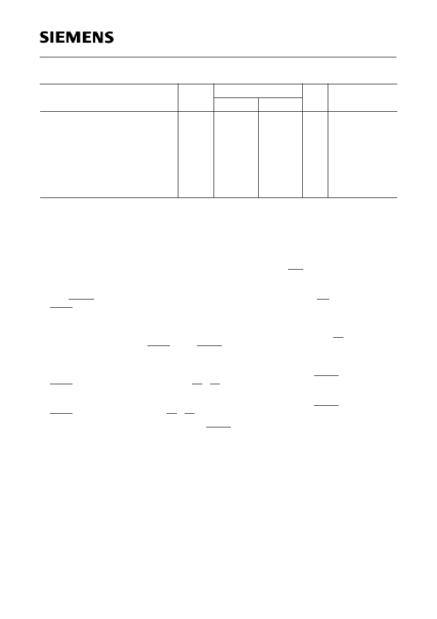
Semiconductor Group
65
09.96
C509-L
Notes :
1) Capacitive loading on ports 0 and 2 may cause spurious noise pulses to be superimposed on the
V
OL
of ALE
and port 1, 3, 4, 5, 6, and 9. The noise is due to external bus capacitance discharging into the port 0 and port
2 pins when these pins make 1-to-0 transitions during bus operation. In the worst case (capacitive loading
> 100 pF), the noise pulse on ALE line may exceed 0.8 V. In such cases it may be desirable to qualify ALE
with a schmitt-trigger, or use an address latch with a schmitt-trigger strobe input.
2) Capacitive loading on ports 0 and 2 may cause the
V
OH
on ALE and PSEN/RDF to momentarily fall below the
0.9
V
CC
specification when the address lines are stabilizing.
3)
I
PD
(power down mode) is measured under following conditions:
EA = RESET =
V
CC
; Port0 = Port7 = Port8 =
V
CC
; XTAL1 = N.C.; XTAL2 =
V
SS
; PE/SWD = OWE =
V
SS
;
HWDP =
V
CC
;
V
AREF
=
V
CC
;
V
AGND
=
V
SS
; all other pins are disconnected.
Hardware power down mode current (
I
PD
) is measured with OWE =
V
CC
or
V
SS
.
4)
I
CC
(active mode) is measured with:
XTAL2 driven with
t
R
/
t
F
= 5 ns ,
V
IL
=
V
SS
+ 0.5 V,
V
IH
=
V
CC
≠ 0.5 V; XTAL1 = N.C.; EA = PE/SWD=
V
CC
;
Port0 =
Port7 =
Port8 =
V
CC
; HWPD =
V
CC
; RESET =
V
SS
; all other pins are disconnected.
I
CC
would be
slightly higher if a crystal oscillator is used.
5)
I
CC
(idle mode) is measured with all output pins disconnected and with all peripherals disabled;
XTAL2 driven with
t
R
/
t
F
= 5 ns,
V
IL
=
V
SS
+ 0.5 V,
V
IH
=
V
CC
≠ 0.5 V; XTAL1 = N.C.; RESET =
V
CC
;
HWPD =
V
CC
; Port0 = Port7 =
Port8 =
V
CC
; EA =
PE/SWD =
V
SS
; all other pins are disconnected;
6)
I
CC
(slow down mode) is measured with all output pins disconnected and with all peripherals disabled;
XTAL2 driven with
t
R
/
t
F
= 5 ns,
V
IL
=
V
SS
+ 0.5 V,
V
IH
=
V
CC
≠ 0.5 V; XTAL1 = N.C.; RESET =
V
CC
;
HWPD =
V
CC
; Port7 =
Port8 =
V
CC
; EA =
PE/SWD =
V
SS
; all other pins are disconnected;
7) Input leakage current for port 0 is measured with RESET =
V
CC
.
8)
I
CC max
at other frequencies is given by:
active mode:TBD
idle mode:TBD
where
f
osc
is the oscillator frequency in MHz.
I
CC
values are given in mA and measured at
V
CC
= 5 V.
9) Typical power supply current (
I
CC typ
) with test conditiones as defined in note 4 and 5 is given by:
active mode, 12 MHz :45 mA
active mode, 16 MHz :72 mA
idle mode, 16 MHz :29 mA
10)Overload conditions occur if the standard operating conditions are exeeded, ie. the voltage on any pin exceeds
the specified range (i.e.
V
OV
>
V
CC
+ 0.5 V or
V
OV
<
V
SS
- 0.5 V). The supply voltage
V
CC
and
V
SS
must remain
within the specified limits. The absolute sum of input currents on all port pins may not exceed 50 mA.
11)Not 100% tested, guaranteed by design characterization.
12)The typical
I
CC
values are periodically measured at
T
A
= +25 ∞C but not 100% tested.
Parameter
Symbol
Limit Values
Unit
Test Condition
typ.
12)
max.
Power supply current:
C509-L, Active mode, 12 MHz
8)
C509-L, Active mode, 16 MHz
8)
C509-L, Idle mode, 12 MHz
8)
C509-L, Idle mode, 16 MHz
8)
C509-L, Slow down mode, 12 MHz
C509-L, Slow down mode, 16 MHz
C509-L, Power Down Mode
I
CC
I
CC
I
CC
I
CC
I
CC
I
CC
I
PD
9)
9)
≠
9)
≠
≠
5
TBD
TBD
TBD
TBD
TBD
TBD
50
mA
mA
mA
mA
mA
mA
µ
A
V
CC
= 5 V,
4)
V
CC
= 5 V,
4)
V
CC
= 5 V,
5)
V
CC
= 5 V,
5)
V
CC
= 5 V,
6)
V
CC
= 5 V,
6)
V
CC
= 2...5.5
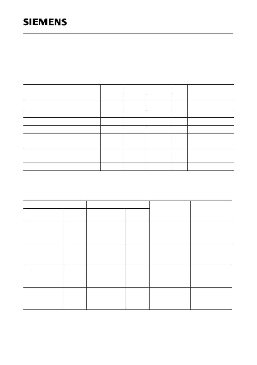
C509-L
Semiconductor Group
66
A/D Converter Characteristics
T
A
= 0 to 70
∞
C
for the SAB-C509
T
A
= ≠ 40 to 85
∞
C for the SAF-C509
V
CC
= 5 V + 10%, ≠ 15%;
V
SS
= 0 V
4 V
V
AREF
V
CC
+0.1 V ;
V
SS
-0.1 V
V
AGND
V
SS
+0.2 V
Notes see next page.
Clock calculation table
Further timing conditions : t
ADC
min = 500 ns = CCP x CLP
t
IN
= 1 / f
OSC
= CLP
t
SC
= t
ADC
x SCP
Parameter
Symbol
Limit Values
Unit
Test Condition
min.
max.
Analog input voltage
V
AIN
V
AGND
V
AREF
V
1)
Sample time
t
S
8
t
IN
512
t
IN
2)
see table below
Conversion time
t
ADCC
48
t
IN
832
t
IN
3)
see table below
Total unadjusted error
TUE
≠
±
2
LSB
4)
Internal resistance of reference
voltage source
R
AREF
≠
t
ADC
/ 250
- 0.25
k
t
ADC
in [ns]
5) 6)
Internal resistance of analog
source
R
ASRC
≠
t
S
/ 500
- 0.25
k
t
S
in [ns]
3) 6)
ADC input capacitance
C
AIN
≠
50
pF
6)
Conversion Clock Selection
Sample Clock Selection
Sample Time
t
S
Conversion Time
t
ADCC
ADCL1 ADCL0
Prescaler
CCP
ADST1 ADST0
Prescaler
SCP
0
0
4
0
0
0
1
1
0
1
1
2
8 x t
IN
16 x t
IN
32 x t
IN
64 x t
IN
48 x t
IN
56 x t
IN
72 x t
IN
104 x t
IN
0
1
8
0
0
0
1
1
0
1
1
4
16 x t
IN
32 x t
IN
64 x t
IN
128 x t
IN
96 x t
IN
112 x t
IN
144 x t
IN
208 x t
IN
1
0
16
0
0
0
1
1
0
1
1
8
32 x t
IN
64 x t
IN
128 x t
IN
256 x t
IN
192 x t
IN
224 x t
IN
288 x t
IN
416 x t
IN
1
1
32
0
0
0
1
1
0
1
1
16
64 x t
IN
128 x t
IN
256 x t
IN
512 x t
IN
384 x t
IN
448 x t
IN
576 x t
IN
832 x t
IN

Semiconductor Group
67
09.96
C509-L
Notes:
1) V
AIN
may exeed V
AGND
or V
AREF
up to the absolute maximum ratings. However, the conversion result in
these cases will be X000
H
or X3FF
H
, respectively.
2) During the sample time the input capacitance
C
AIN
can be charged/discharged by the external source. The
internal resistance of the analog source must allow the capacitance to reach their final voltage level within t
S
.
After the end of the sample time t
S
, changes of the analog input voltage have no effect on the conversion result.
3) This parameter includes the sample time t
S
, the time for determining the digital result and the time for the
calibration. Values for the conversion clock f
ADC
depend on programming and can be taken from the table
below.
4) T
UE
is tested at V
AREF
= 5.0 V, V
AGND
= 0 V, V
CC
= 4.9 V. It is guaranteed by design characterization for all
other voltages within the defined voltage range.
If an overload condition occurs on maximum 2 not selected analog input pins and the absolute sum of input
overload currents on all analog input pins does not exceed 10 mA, an additional conversion error of 1/2 LSB
is permissible.
5) During the conversion the ADC's capacitance must be repeatedly charged or discharged. The internal
resistance of the reference source must allow the capacitance to reach their final voltage level within the
indicated time. The maximum internal resistance results from the programmed conversion timing.
6) Not 100% tested, but guaranteed by design characterization.
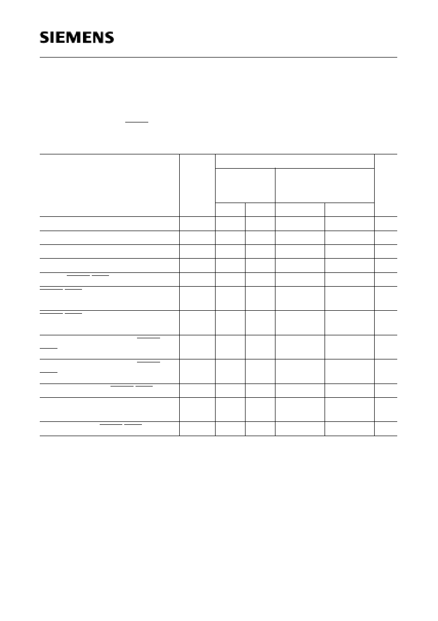
C509-L
Semiconductor Group
68
AC Characteristics
*)
Interfacing the C509-L to devices with float times up to 20 ns is permissible. This limited bus contention will not
cause any damage to port 0 drivers.
V
CC
= 5 V + 10%, ≠ 15%;
V
SS
= 0 V
T
A
= 0 to 70
∞
C
for the SAB-C509
T
A
= ≠ 40 to 85
∞
C for the SAF-C509
(
C
L
for port 0, ALE and PSEN outputs = 100 pF;
C
L
for all other outputs = 80 pF)
Program Memory Characteristics
Parameter
Symbol
Limit Values
Unit
16-MHz clock
Duty Cycle
0.4 to 0.6
Variable Clock
1/CLP = 3.5 MHz to
16 MHz
min.
max.
min.
max.
ALE pulse width
t
LHLL
48
≠
CLP-15
≠
ns
Address setup to ALE
t
AVLL
10
≠
TCL
Hmin
-15
≠
ns
Address hold after ALE
t
LLAX
10
≠
TCL
Hmin
-15
≠
ns
Address to valid instruction in
t
LLIV
≠
75
≠
2 CLP-50
ns
ALE to PSEN/RDF
t
LLPL
10
≠
TCL
Lmin
-15
≠
ns
PSEN/RDF pulse width
t
PLPH
73
≠
CLP+
TCL
Hmin
-15
≠
ns
PSEN/RDF to valid instruction in
t
PLIV
≠
38
≠
CLP+
TCL
Hmin
-50
ns
Input instruction hold after PSEN/
RDF
t
PXIX
0
≠
0
≠
ns
Input instruction float after PSEN/
RDF
t
PXIZ
*)
≠
15
≠
TCL
Lmin
-10
ns
Address valid after PSEN/RDF
t
PXAV
*)
20
≠
TCL
Lmin
-5
≠
ns
Address to valid instruction in
t
AVIV
≠
95
≠
2 CLP+
TCL
Hmin
-55
ns
Address float to PSEN/RDF
t
AZPL
- 5
- 5
≠
ns
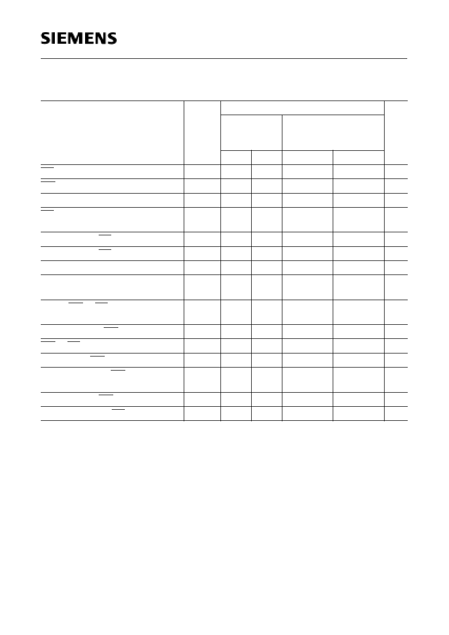
Semiconductor Group
69
09.96
C509-L
External Data Memory Characteristics
Parameter
Symbol
Limit Values
Unit
16-MHz clock
Duty Cycle
0.4 to 0.6
Variable Clock
1/CLP= 3.5 MHz to
16 MHz
min.
max.
min.
max.
RD pulse width
t
RLRH
158
≠
3 CLP-30
≠
ns
WR pulse width
t
WLWH
158
≠
3 CLP-30
≠
ns
Address hold after ALE
t
LLAX2
48
≠
CLP -15
≠
ns
RD to valid data in
t
RLDV
≠
100
≠
2 CLP+
TCL
Hmin
-50
ns
Data hold after RD
t
RHDX
0
0
≠
ns
Data float after RD
t
RHDZ
≠
51
≠
CLP-12
ns
ALE to valid data in
t
LLDV
≠
200
≠
4 CLP-50
ns
Address to valid data in
t
AVDV
≠
200
≠
4 CLP+
TCL
Hmin
-75
ns
ALE to WR or RD
t
LLWL
73
103
CLP+
TCL
Lmin
-15
CLP+
TCL
Lmin
+15
ns
Address valid to WR
t
AVWL
95
≠
2 CLP-30
≠
ns
WR or RD high to ALE high
t
WHLH
10
40
TCL
Hmin
-15
TCL
Hmin
+15 ns
Data valid to WR transition
t
QVWX
5
≠
TCL
Lmin
-20
≠
ns
Data setup before WR
t
QVWH
163
≠
3 CLP+
TCL
Lmin
-50
≠
ns
Data hold after WR
t
WHQX
5
≠
TCL
Hmin
-20
≠
ns
Address float after RD
t
RLAZ
≠
0
≠
0
ns
C509-L
Semiconductor Group
70
Note: The 16 MHz values in the tables are given as an example for a typical duty cycle variation of
the oscillator clock from 0.4 to 0.6.
External Clock Drive XTAL2
Parameter
Symbol
CPU Clock = 16 MHz
Duty cycle 0.4 to 0.6
Variable CPU Clock
1/CLP = 3.5 to 16 MHz
Unit
min.
max.
min.
max.
Oscillator period
CLP
62.5
62.5
62.5
285
ns
High time
TCL
H
25
≠
25
CLP-TCL
L
ns
Low time
TCL
L
25
≠
25
CLP-TCL
H
ns
Rise time
t
R
≠
10
≠
10
ns
Fall time
t
F
≠
10
≠
10
ns
Oscillator duty cycle
DC
0.4
0.6
25 / CLP
1 - 25 / CLP
≠
Clock cycle
TCL
25
37.5
CLP * DC
min
CLP * DC
max
ns
Semiconductor Group
71
09.96
C509-L
Figure 36
Program Memory Read Cycle
Figure 37
Data Memory Read Cycle
C509-L
Semiconductor Group
72
Figure 38
Data Memory Write Cycle
Figure 39
External Clock Drive Drive XTAL2
Semiconductor Group
73
09.96
C509-L
Figure 40
AC Testing: Input, Output Waveforms
Figure 41
AC Testing: Float Waveforms
Figure 42
Recommended Oscillator Circuits for Crystal Oscillators up to 16 MHz
AC Inputs during testing are driven at
V
CC
- 0.5 V for a logic '1' and 0.45 V for a logic '0'.
Timing measurements are made at
V
IHmin
for a logic '1' and
V
ILmax
for a logic '0'.
For timing purposes a port pin is no longer floating when a 100 mV change from load voltage
occurs and begins to float when a 100 mV change from the loaded
V
OH
/
V
OL
level occurs.
I
OL
/
I
OH
±
20 mA