 | –≠–ª–µ–∫—Ç—Ä–æ–Ω–Ω—ã–π –∫–æ–º–ø–æ–Ω–µ–Ω—Ç: C541U | –°–∫–∞—á–∞—Ç—å:  PDF PDF  ZIP ZIP |

'DWD 6KHHW
0LFURFRPSXWHU &RPSRQHQWV
%LW &026 0LFURFRQWUROOHU
&8
ht
tp:
//ww
w
.si
em
en
s.
d
Sem
ic
ondu
ct
or
/

Edition 05.99
This edition was realized using the software system FrameMaker
Æ
.
Published by Siemens AG,
Bereich Halbleiter, Marketing-
Kommunikation, Balanstraþe 73,
81541 M¸nchen
© Siemens AG 6/2/99.
All Rights Reserved.
Attention please!
As far as patents or other rights of third parties are concerned, liability is only assumed for components, not for applications, pro-
cesses and circuits implemented within components or assemblies.
The information describes the type of component and shall not be considered as assured characteristics.
Terms of delivery and rights to change design reserved.
For questions on technology, delivery and prices please contact the Semiconductor Group Offices in Germany or the Siemens Com-
panies and Representatives worldwide (see address list).
Due to technical requirements components may contain dangerous substances. For information on the types in question please con-
tact your nearest Siemens Office, Semiconductor Group.
Siemens AG is an approved CECC manufacturer.
Packing
Please use the recycling operators known to you. We can also help you ≠ get in touch with your nearest sales office. By agreement
we will take packing material back, if it is sorted. You must bear the costs of transport.
For packing material that is returned to us unsorted or which we are not obliged to accept, we shall have to invoice you for any costs
incurred.
Components used in life-support devices or systems must be expressly authorized for such purpose!
C541U Data Sheet
Revision History :
05.99
Previous Releases :
10.97(Original Version)
Page
(10.97
version)
Page
(05.99
version)
Subjects (changes since last revision)
All sections
All sections
1
2
2
2
4
5
6 to 9
21
22
24
31
38
39 to 40
43
43
43
-
44
44
44
44
45
45
46
59
61
63
All sections
All sections
1
2
2
2
4
5
5 to 8
20
22
24
31
37
38 to 39
42
42
42
42
43
43
43
43
44
44
45
58
60
61
All references to C540U is removed.
V
CC
is changed to
V
DD
.
Compliant to USB Specification "Rev 1.0".
Power supply voltage range changed to 4.25V to 5.5V.
Line "* P-SDIP-52 package ..." is added.
Table 1 is removed and replaced by "Ordering Information".
Figure 3; pin 2 is changed to ECAP.
Figure 4 is removed.
Table 1; column P-SDIP-52 is deleted and any references to P-SDIP-52 is also
removed, the definition of pin 2 is changed to ECAP.
Table 3; modified with addition of bit DRVI in GEPIR register.
Table 4; modified with addition of bits DRVIE and XVREG in DPWDR register.
First sentence; reference to P-SDIP-52 is removed.
Figure 16 is modified to include DRVI and DRVIE.
Figure 22 is removed.
Table 8; column P-SDIP-52 is removed.
"Absolute Maximum Ratings" is changed to tabular form.
Fifth line; "During overload conditions ..." changed to "During absolute
maximum rating conditons ...".
"Operating Conditions" is added.
V
DD
is changed to 4.25V to 5.5V (5V +10%, -15%)
"
V
CC
= 5 V + 10% ... " is replaced by "(Operating Conditions apply)".
V
IH min
of EA is changed to 0.6
V
DD
.
V
OL max
of Port 0 is changed to 0.6 V.
I
IL max
is changed to -60 µA.
Values for
I
DD
(active and idle mode) and
I
PD
Notes (6); modified.
"
V
CC
= 5 V + 10% ... " is replaced by "(Operating Conditions apply)".
"
V
CC
= 5 V + 10% ... " is replaced by "(Operating Conditions apply)".
Figure 37 is added.
Figure 40 is removed.
Semiconductor Group
1
C541U
8-Bit CMOS Microcontroller
Advance Information
C541U
∑
Enhanced 8-bit C500 CPU
≠ Full software/toolset compatible to standard 80C51/80C52 microcontrollers
∑
12 MHz external operating frequency
≠ 500 ns instruction cycle
∑
Built-in PLL for USB synchronization
∑
On-chip OTP program memory
≠ 8K byte
≠ Alternatively up to 64K byte external program memory
≠ Optional memory protection
∑
On-chip USB module
≠ Compliant to USB specification Rev1.0
≠ Full speed or low speed operation
≠ Five endpoints : one bidirectional control endpoint
four versatile programmable endpoints
≠ Registers are located in special function register area
≠ On-chip USB transceiver
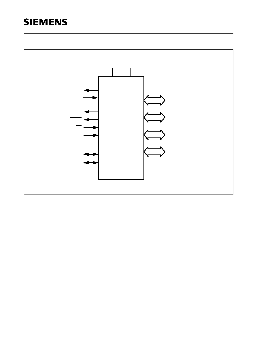
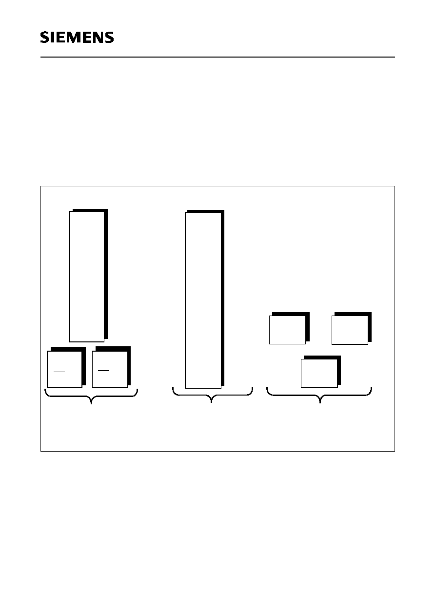
Figure 1
C541U Functional Units
SSC
T0
T1
CPU
Port 0
Port 1
Port 2
Port 3
I/O
I/O
OTP Prog. Memory
Watchdog
I/O
I/O
O
n
-C
hi
p Emula
t
ion Suppo
rt Modul
e
Module
RAM
256
◊
8
Timer
Oscillator
Watchdog
Power
Saving
Modes
USB Transceiver
D+
D-
USB
8k
◊
8

Semiconductor Group
2
C541U
Features (continued) :
∑
Up to 64K byte external data memory
∑
256 byte on-chip RAM
∑
Four parallel I/O ports
≠ P-LCC-44 package :
three 8-bit ports and one 6-bit port
≠ P-SDIP-52* package : four 8-bit ports
≠ LED current drive capability for 3 pins (10 mA)
∑
Two 16-bit timer/counters (C501 compatible)
∑
SSC synchronous serial interface (SPI compatible)
≠ Master and slave capable
≠ Programmable clock polarity / clock-edge to data phase relation
≠ LSB/MSB first selectable
≠ 1.5 MBaud transfer rate at 12 MHz operating frequency
∑
7 interrupt sources (2 external, 5 internal with 2 USB interrupts) selectable at 2 priority levels
∑
Enhanced fail safe mechanisms
≠ Programmable watchdog timer
≠ Oscillator watchdog
∑
Power saving modes
≠ idle mode
≠ software power down mode with wake-up capability through INT0 pin or USB
∑
On-chip emulation support logic (Enhanced Hooks Technology
TM
)
∑
P-LCC-44 and P-SDIP-52* packages
∑
Power supply voltage range : 4.25V to 5.5V
∑
Temperature Range :
T
A
= 0 to 70
∞
C
* P-SDIP-52 package is available on specific request from customer
Semiconductor Group
3
C541U
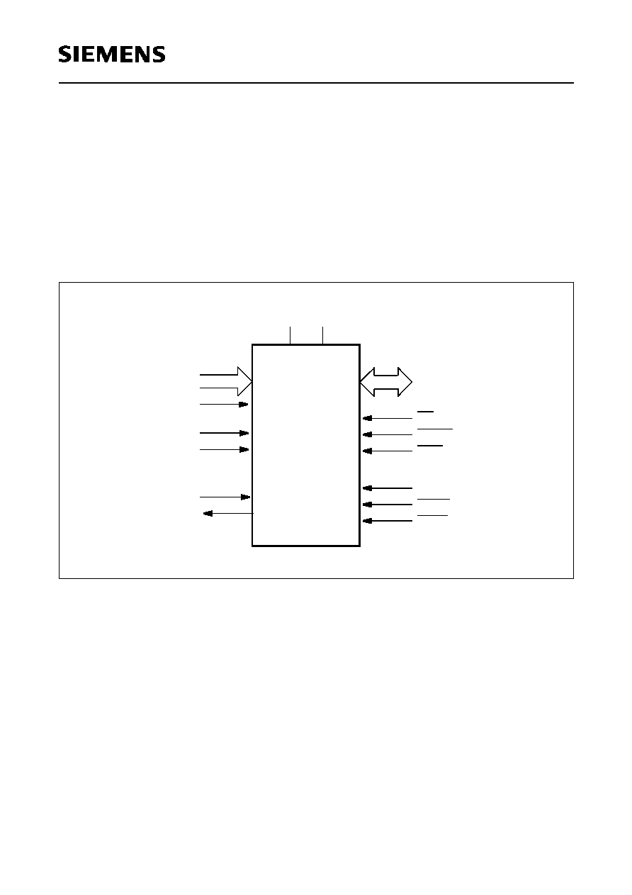
Figure 2
Logic Symbol
Port 0
8-bit Digital I/O
RESET
EA
ALE
PSEN
XTAL2
XTAL1
Port 1
6-bit Digital I/O
Port 2
8-bit Digital I/O
Port 3
8-bit Digital I/O
V
SS
V
DD
D+
D-
C541U
Semiconductor Group
4
C541U
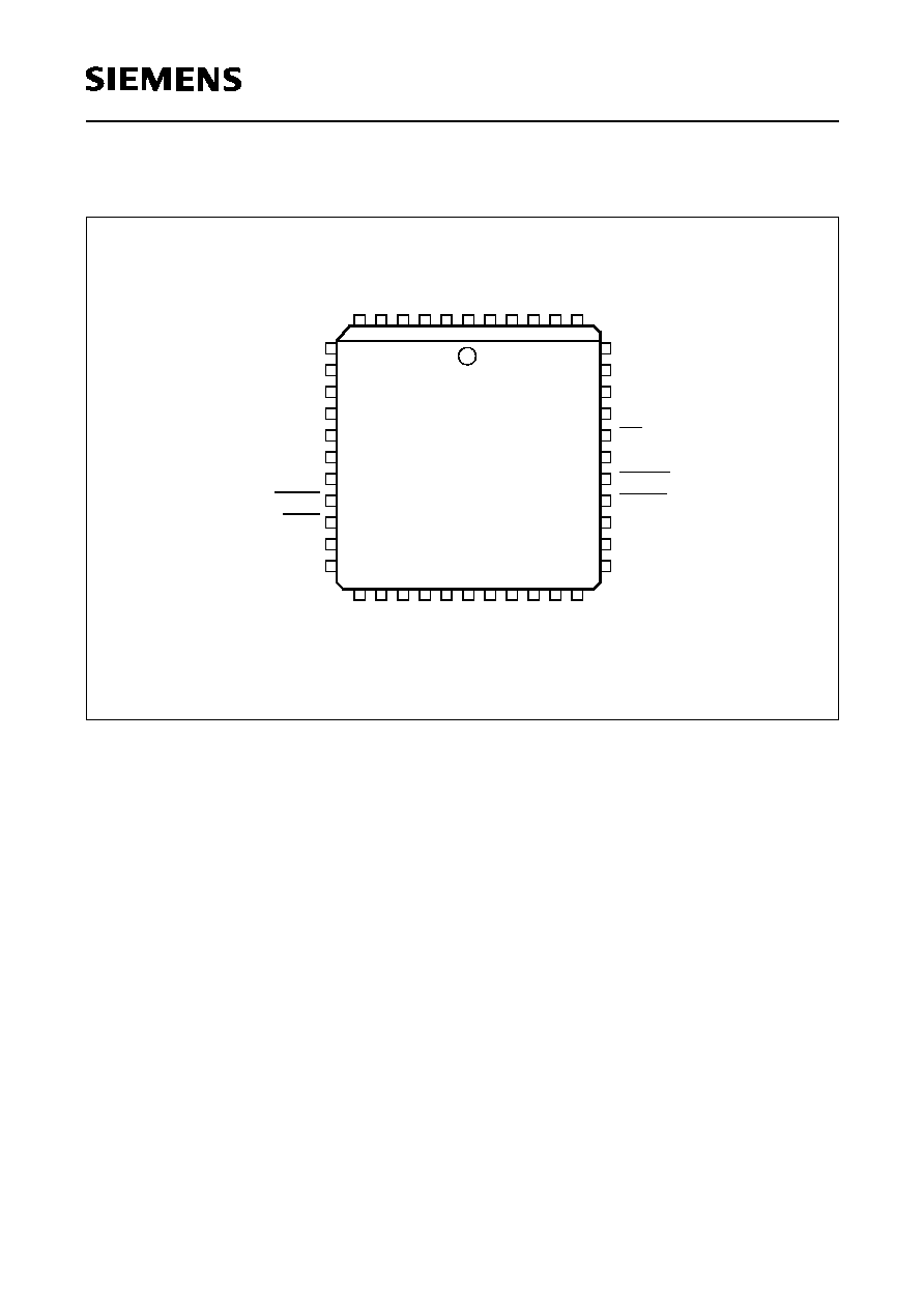
Figure 3
Pin Configuration (Top View)
P1.5/
S
LS
P1.3/SRI
6
7
8
9
10
11
12
13
14
15
16
17
5
4
3
2
1
44 43 42 41 40
39
38
37
36
35
34
33
32
31
30
29
18 19 20 21 22 23 24 25 26 27
P1.1/
L
E
D
1
P1.0/
L
E
D
0
D-
D+
ECAP
V
DD
U
P1.2/SCLK
V
DD
V
SS
P3.0/LED2
P3.1/DADD
P3.2/INT0
P3.3/INT1
P3.4/T0
P3.5/T1
P
3
.
6
/WR
P3.7/RD
XTAL2
XTAL1
V
SS
V
DD
P2.0/A8
P2.1/A9
P2.2/A10
P2.3/A11
P2.4/A12
RESET
P0.3/
A
D3
P0.2/
A
D2
P0.1/
A
D1
P0.0/
A
D0
P0.4/AD4
P0.5/AD5
P0.6/AD6
P0.7/AD7
EA
P1.4/STO
PSEN
P2.7/A15
P2.6/A14
P2.5/A13
ALE
28
C541U
Semiconductor Group
5
C541U
Table 1
Pin Definitions and Functions
Symbol
Pin
Numbers
I/O*) Function
P-LCC-44
D+
3
I/O
USB D+ Data Line
The pin D+ can be directly connected to USB cable (transceiver
is integrated on-chip).
D-
4
I/O
USB D- Data Line
The pin D- can be directly connected to USB cable (transceiver is
integrated on-chip).
P1.0 - P1.4
5 - 7,
12, 34, 44
5
6
7
12
34
44
I/O
Port 1
is an 6-bit quasi-bidirectional I/O port with internal pullup
resistors. Port 1 pins that have 1's written to them are pulled high
by the internal pullup resistors, and in that state can be used as
inputs. As inputs, port 1 pins being externally pulled low will
source current (
I
IL
, in the DC characteristics) because of the
internal pullup resistors.
Port 1 also contains two outputs with LED drive capability as well
as the four pins of the SSC. The pins with LED drive capability are
able to sink current up to 10 mA. The output latch corresponding
to a secondary function must be programmed to a one (1) for that
function to operate (except when used for the compare functions).
The secondary functions are assigned to the port 1 pins as
follows :
P1.0 / LED0 LED0 output
P1.1 / LED1 LED1 output
P1.2 / SCLK SSC Master Clock Output /
SSC Slave Clock Input
P1.3 / SRI
SSC Receive Input
P1.4 / STO
SSC Transmit Output
P1.5 / SLS
SSC Slave Select Inp.
RESET
10
I
RESET
A high level on this pin for the duration of two machine cycles
while the oscillator is running resets the C541U. A small internal
pulldown resistor permits power-on reset using only a capacitor
connected to V
DD
.
*) I = Input
O = Output
Semiconductor Group
6
C541U
P3.0 - P3.7
11, 13 - 19
11
13
14
15
16
17
18
19
I/O
Port 3
is an 8-bit quasi-bidirectional I/O port with internal pullup
resistors. Port 3 pins that have 1's written to them are pulled high
by the internal pullup resistors, and in that state can be used as
inputs. As inputs, port 3 pins being externally pulled low will
source current (
I
IL
, in the DC characteristics) because of the
internal pullup resistors. Port 3 also contains the interrupt, timer,
serial port and external memory strobe pins that are used by
various options. The pin with LED drive capability are able to sink
current up to 10 mA. The output latch corresponding to a
secondary function must be programmed to a one (1) for that
function to operate. The secondary functions are assigned to the
pins of port 3, as follows:
P3.0 / LED2
LED2 output
P3.1 / DADD
Device attached input
P3.2 / INT0
External interrupt 0 input /
timer 0 gate control input
P3.3 / INT1
External interrupt 1 input /
timer 1 gate control input
P3.4 / T0
Timer 0 counter input
P3.5 / T1
Timer 1 counter input
P3.6 / WR
WR control output; latches the
data byte from port 0 into the
external data memory
P3.7 / RD
RD control output; enables the
external data memory
XTAL2
20
≠
XTAL2
is the output of the inverting oscillator amplifier. This pin is used
for the oscillator operation with crystal or ceramic resonator.
XTAL1
21
≠
XTAL1
is the input to the inverting oscillator amplifier and input to the
internal clock generator circuits.
To drive the device from an external clock source, XTAL1 should
be driven, while XTAL2 is left unconnected.
Minimum and
maximum high and low times as well as rise/fall times specified in
the AC characteristics must be observed.
*) I = Input
O = Output
Table 1
Pin Definitions and Functions (cont'd)
Symbol
Pin
Numbers
I/O*) Function
P-LCC-44
Semiconductor Group
7
C541U
P2.0 - P2.7
24 - 31
I/O
Port 2
is an 8-bit quasi-bidirectional I/O port with internal pullup
resistors. Port 2 pins that have 1's written to them are pulled high
by the internal pullup resistors, and in that state can be used as
inputs. As inputs, port 2 pins being externally pulled low will
source current (
I
IL
, in the DC characteristics) because of the
internal pullup resistors.
Port 2 emits the high-order address byte during fetches from
external program memory and during accesses to external data
memory that use 16-bit addresses (MOVX @DPTR). In this
application it uses strong internal pullup resistors when issuing
1's. During accesses to external data memory that use 8-bit
addresses (MOVX @Ri), port 2 issues the contents of the P2
special function register.
PSEN
32
O
The Program Store Enable
output is a control signal that enables the external program
memory to the bus during external fetch operations. It is activated
every three oscillator periods except during external data memory
accesses. The signal remains high during internal program
execution.
ALE
33
O
The Address Latch enable
output is used for latching the address into external memory
during normal operation. It is activated every three oscillator
periods except during an external data memory access.
EA
35
I
External Access Enable
When held high, the C541U executes instructions from the
internal OTP program memory as long as the PC is less than
2000H for the C541U. When held low, the C541U fetches all
instructions from external program memory. For the C541U-L this
pin must be tied low.
P0.0 - P0.7
43 - 36
I/O
Port 0
is an 8-bit open-drain bidirectional I/O port. Port 0 pins that have
1's written to them float, and in that state can be used as high-
impedance inputs. Port 0 is also the multiplexed low-order
address and data bus during accesses to external program and
data memory. In this application it uses strong internal pullup
resistors when issuing 1's.
*) I = Input
O = Output
Table 1
Pin Definitions and Functions (cont'd)
Symbol
Pin
Numbers
I/O*) Function
P-LCC-44
Semiconductor Group
8
C541U
ECAP
2
≠
External Capacitor
This pin is required to be connected to an external capacitor
which is connected to
V
SS
. The recommended value for the
capacitor is 6.8 nF.
V
DDU
1
≠
Supply voltage
for the on-chip USB transceiver circuitry
V
DD
8, 23
≠
Supply voltage
for ports and internal logic circuitry during normal, idle, and power
down mode.
V
SS
9, 22
≠
Ground (0V)
during normal, idle, and power down mode.
*) I = Input
O = Output
Table 1
Pin Definitions and Functions (cont'd)
Symbol
Pin
Numbers
I/O*) Function
P-LCC-44
Semiconductor Group
9
C541U
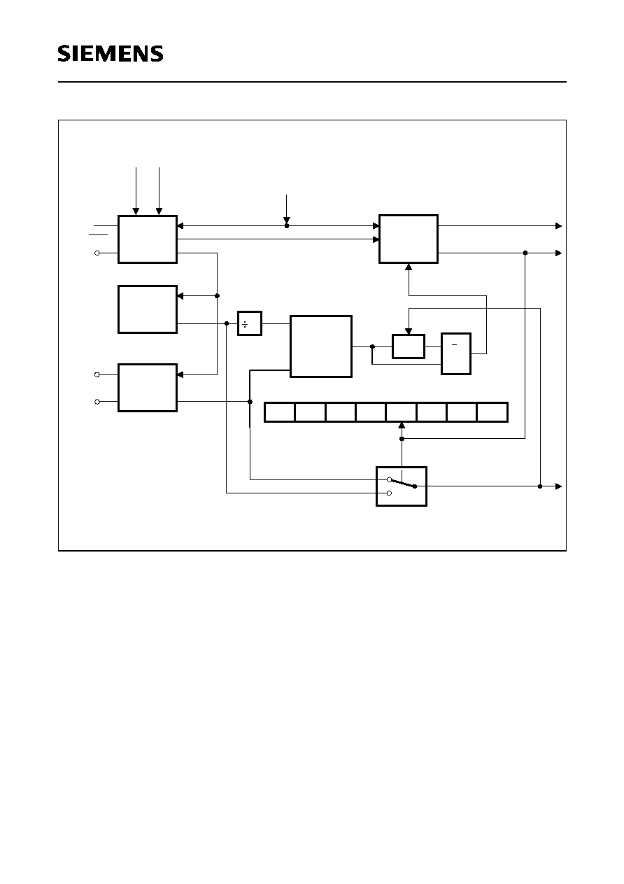
Figure 4
Block Diagram of the C541U
Port 0
8-bit digit. I/O
Port 2
8-bit digit. I/O
Port 3
8-bit digit. I/O
Port 0
Port 1
Port 2
Port 3
OSC & Timing
CPU
Timer 0
Interrupt Unit
XTAL2
XTAL1
RESET
ALE
PSEN
EA
Port 1
6-bit digit. I/O
256 x 8
RAM
Timer
Progr. Watchdog
Emulation
Support
Logic
Oscillator Watchdog
OTP
Timer 1
SSC (SPI) Interface
USB
Module
Memory
D+
D-
C541U
8k x 8
PLL
Tran
scei
v
er
Semiconductor Group
10
C541U
CPU
The C541U is efficient both as a controller and as an arithmetic processor. It has extensive facilities
for binary and BCD arithmetic and excels in its bit-handling capabilities. Efficient use of program
memory results from an instruction set consisting of 44 % one-byte, 41 % two-byte, and 15% three-
byte instructions. With a 12 MHz crystal, 58% of the instructions are executed in 500ns.
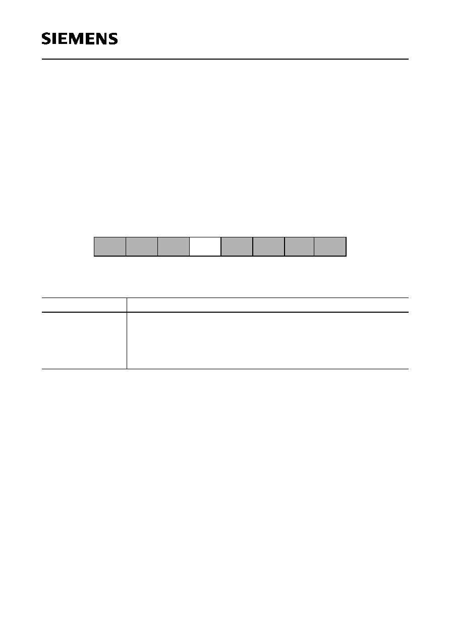
Special Function Register PSW (Address D0H)
Reset Value : 00H
Bit
Function
CY
Carry Flag
Used by arithmetic instruction.
AC
Auxiliary Carry Flag
Used by instructions which execute BCD operations.
F0
General Purpose Flag
RS1
RS0
Register Bank Select Control Bits
These bits are used to select one of the four register banks.
OV
Overflow Flag
Used by arithmetic instruction.
F1
General Purpose Flag
P
Parity Flag
Set/cleared by hardware after each instruction to indicate an odd/even
number of "one" bits in the accumulator, i.e. even parity.
CY
AC
F0
RS1
RS0
OV
F1
P
D0H
PSW
D7H
D6H
D5H
D4H
D3H
D2H
D1H
D0H
Bit No.
MSB
LSB
RS1
RS0
Function
0
0
Bank 0 selected, data address 00H-07H
0
1
Bank 1 selected, data address 08H-0FH
1
0
Bank 2 selected, data address 10H-17H
1
1
Bank 3 selected, data address 18H-1FH
Semiconductor Group
11
C541U
Memory Organization
The C541U CPU manipulates operands in the following four address spaces:
≠ 8KByte on-chip OTP program memory
≠ Totally up to 64 Kbyte internal/external program memory
≠ up to 64 Kbyte of external data memory
≠ 256 bytes of internal data memory
≠ a 128 byte special function register area
Figure 5 illustrates the memory address spaces of the C541U.
Figure 5
C541U Memory Map Memory Map
FFFFH
2000H
1FFFH
0000H
"Code Space"
Internal
(EA = 1)
External
(EA = 0)
"internal Data Space"
indirect
direct
addr.
7FH
00H
Internal
RAM
Special
Function
Register
80H
FFH
80H
FFH
addr.
External
Internal
RAM
"External Data Space"
0000H
FFFFH
External
Semiconductor Group
12
C541U
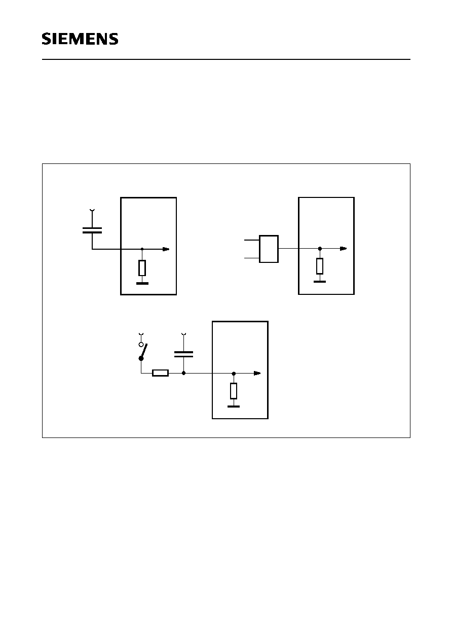
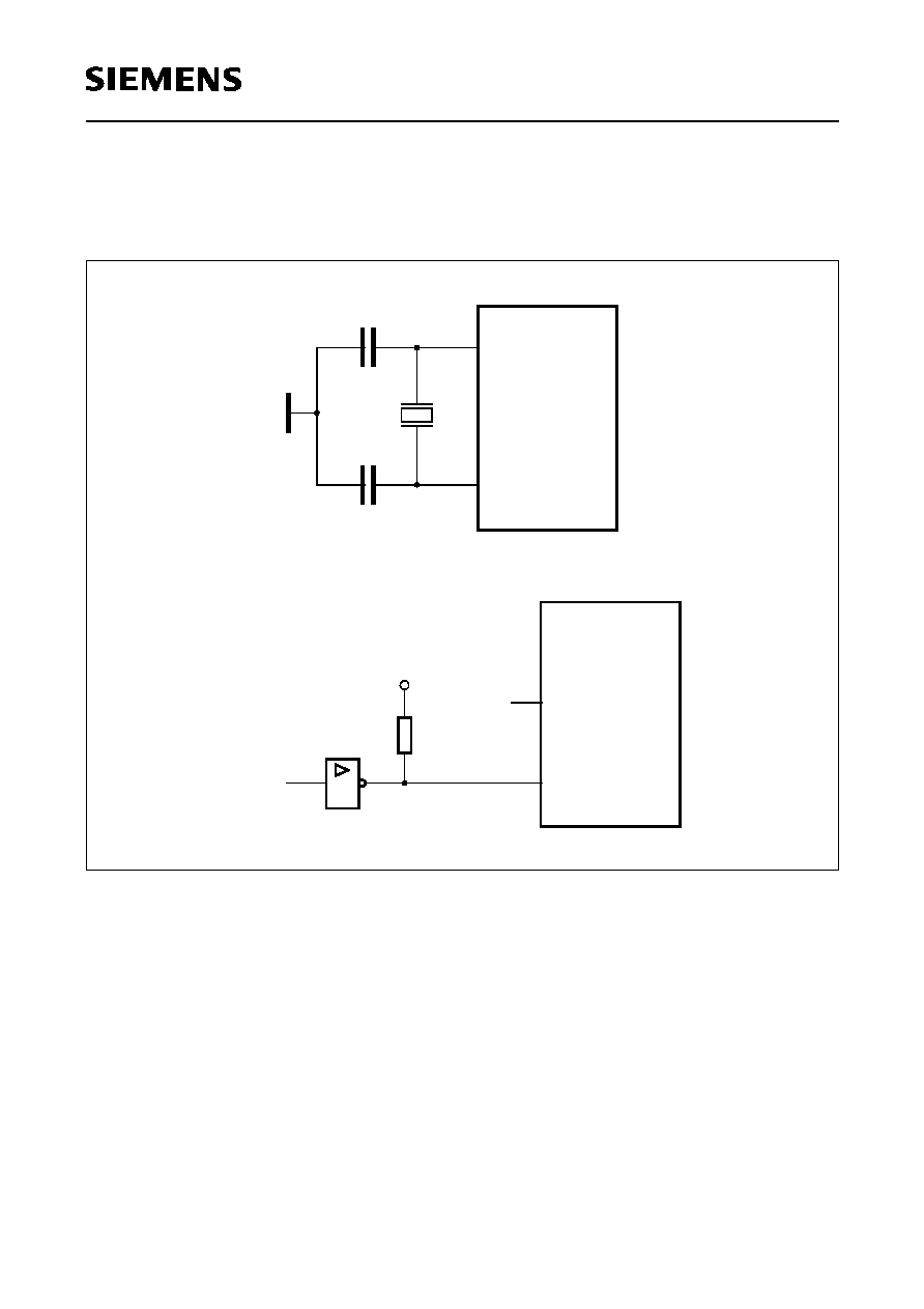
Reset and System Clock
The reset input is an active high input at pin RESET. Since the reset is synchronized internally, the
RESET pin must be held high for at least two machine cycles (12 oscillator periods) while the
oscillator is running. A pulldown resistor is internally connected to
V
SS
to allow a power-up reset with
an external capacitor only. An automatic reset can be obtained when
V
DD
is applied by connecting
the RESET pin to
V
DD
via a capacitor. Figure 6 shows the possible reset circuitries.
Figure 6
Reset Circuitries
RESET
+
a)
RESET
b)
&
RESET
c)
V
DD
+
V
DD
V
DD
C541U
C541U
C541U
Semiconductor Group
13
C541U
The oscillator and clock generation circuitry of the C541U is shown in figure 5-7. The crystal
oscillator generates the system clock for the microcontroller. The USB module can be provided with
the following clocks :
≠ Full speed operation : 48 MHz with a data rate of 12 Mbit/s
≠ Low speed operation : 6 MHz with a data rate of 1.5 Mbit/s
The low speed clock is generated by a dividing the system clock by 2. The full speed clock is
generated by a PLL, which multiplies the system clock by a fix factor of 4. This PLL can be enabled
or disabled by bit PCLK of SFR DCR. Depending on full or low speed operation of the USB bit
SPEED of SFR has to be set or cleared for the selection of the USB clock. Bit UCLK is a general
enable bit for the USB clock.
Figure 7
Block Diagram of the Clock Generation Circuitry
XTAL1
Crystal
Oscillator
12
XTAL2
Pin
Pin
System clock
of the
microcontroller
6 MHz
MHz
UCLK
DCR.1
PLL
x 4
48 MHz
0
1
Divider
by 2
SPEED
DCR.7
to USB
Module
DCR.0
PCLK
Enable
12 MHz
C541U
Semiconductor Group
14
C541U
The clock generator provides the internal clock signals to the chip. These signals define the internal
phases, states and machine cycles. Figure 8 shows the recommended oscillator circuits for crystal
and external clock operation.
Figure 8
Recommended Oscillator Circuitries
XTAL1
XTAL2
C
C
12
MHz
C = 20pF
±
10pF for crystal operation
C541U
External
Clock
Signal
V
DD
N.C.
XTAL2
XTAL1
C541U
Semiconductor Group
15
C541U
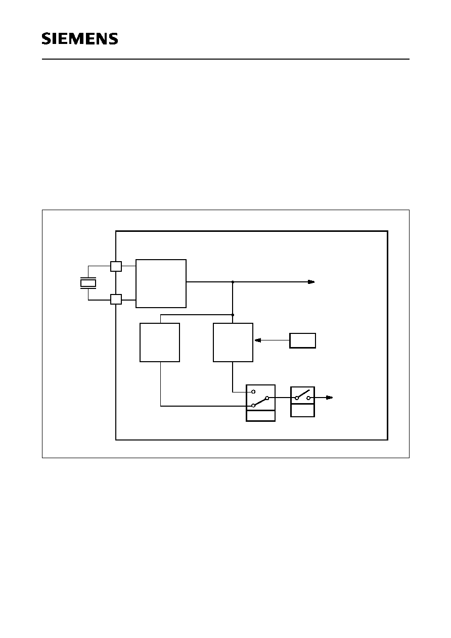
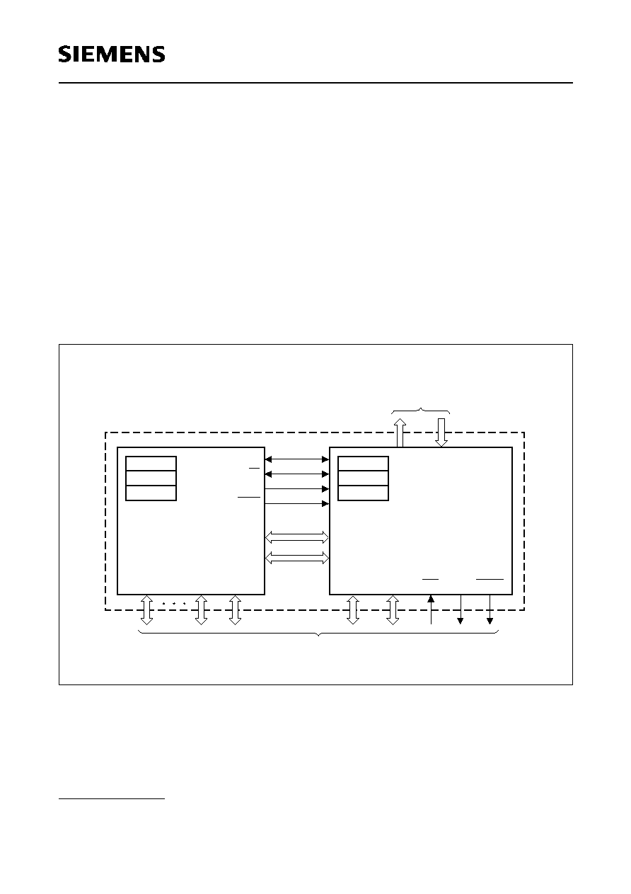
Enhanced Hooks Emulation Concept
The Enhanced Hooks Emulation Concept of the C500 microcontroller family is a new, innovative
way to control the execution of C500 MCUs and to gain extensive information on the internal
operation of the controllers. Emulation of on-chip ROM based programs is possible, too.
Each production chip has built-in logic for the supprt of the Enhanced Hooks Emulation Concept.
Therefore, no costly bond-out chips are necessary for emulation. This also ensure that emulation
and production chips are identical.
The Enhanced Hooks Technology
TM
1)
, which requires embedded logic in the C500 allows the C500
together with an EH-IC to function similar to a bond-out chip. This simplifies the design and reduces
costs of an ICE-system. ICE-systems using an EH-IC and a compatible C500 are able to emulate
all operating modes of the different versions of the C500 microcontrollers. This includes emulation
of ROM, ROM with code rollover and ROMless modes of operation. It is also able to operate in
single step mode and to read the SFRs after a break.
Figure 9
Basic C500 MCU Enhanced Hooks Concept Configuration
Port 0, port 2 and some of the control lines of the C500 based MCU are used by Enhanced Hooks
Emulation Concept to control the operation of the device during emulation and to transfer
informations about the programm execution and data transfer between the external emulation
hardware (ICE-system) and the C500 MCU.
1 "Enhanced Hooks Technology" is a trademark and patent of Metalink Corporation licensed to Siemens.
MCS02647
SYSCON
PCON
TCON
RESET
EA
PSEN
ALE
Port 0
Port 2
I/O Ports
Optional
Port 3
Port 1
C500
MCU
Interface Circuit
Enhanced Hooks
RPort 0
RPort 2
RTCON
RPCON
RSYSCON
TEA
TALE TPSEN
EH-IC
Target System Interface
ICE-System Interface
to Emulation Hardware
Semiconductor Group
16
C541U
Special Function Registers
The registers, except the program counter and the four general purpose register banks, reside in
the special function register area. The special function register area consists of two portions: the
standard special function register area and the mapped special function register area. One special
function register of the C541U (PCON1) is located in the mapped special function register area. All
other SFRs are located in the standard special function register area.
For accessing PCON1 in the mapped special function register area, bit RMAP in special function
register SYSCON must be set.
Special Function Register SYSCON (Address B1H)
Reset Value : XX10XXXXB
As long as bit RMAP is set, a mapped special function register can be accessed. This bit is not
cleared by hardware automatically. Thus, when non-mapped/mapped registers are to be accessed,
the bit RMAP must be cleared/set by software, respectively each.
The registers, except the program counter and the four general purpose register banks, reside in the
special function register area. All SFRs with addresses where address bits 0-2 are 0 (e.g. 80H,
88H, 90H, 98H, ..., F8H, FFH) are bitaddressable.
The 75 special function registers (SFRs) in the SFR area include pointers and registers that provide
an interface between the CPU and the other on-chip peripherals. The SFRs of the C541U are listed
in table 2 to table 4. In table 2 they are organized in groups which refer to the functional blocks of
the C541U. Table 4 and table 4 illustrate the contents of the SFRs in numeric order of their
addresses.
Bit
Function
RMAP
Special function register map bit
RMAP = 0 : The access to the non-mapped (standard) special function
register area is enabled.
RMAP = 1 : The access to the mapped special function register area
(PCON1) is enabled.
7
6
5
4
3
2
1
0
EALE
RMAP
≠
B1H
SYSCON
Bit No.
MSB
LSB
≠
≠
≠
≠
≠
The functions of the shaded bits are not described in this section.
Semiconductor Group
17
C541U
Table 2
Special Function Registers - Functional Blocks
Block
Symbol
Name
Address
Contents after
Reset
CPU
ACC
B
DPH
DPL
PSW
SP
VR0
VR1
VR2
SYSCON
Accumulator
B Register
Data Pointer, High Byte
Data Pointer, Low Byte
Program Status Word Register
Stack Pointer
Version Register 0
Version Register 1
Version Register 2
System Control Register
E0H
1)
F0H
1)
83H
82H
D0H
1)
81H
FCH
FDH
FEH
B1H
00H
00H
00H
00H
00H
07H
C5H
C1H
YYH
3)
XX10XXXXB
2)
Interrupt
System
IEN0
IEN1
IP0
IP1
ITCON
Interrupt Enable Register 0
Interrupt Enable Register 1
Interrupt Priority Register 0
Interrupt Priority Register 1
External Interrupt Trigger Condition Register
A8H
1)
A9H
B8H
1)
B9H
)
9AH
0XXX0000B
2)
XXXXX000B
2)
XXXX0000B
2)
XXXXX000B
2)
XXXX1010B
2)
Ports
P0
P1
P2
P3
Port 0
Port 1
Port 2
Port 3
80H
1)
90H
1)
A0H
1)
B0H
1)
FFH
FFH
FFH
FFH
Timer 0 /
Timer 1
TCON
TH0
TH1
TL0
TL1
TMOD
Timer 0/1 Control Register
Timer 0, High Byte
Timer 1, High Byte
Timer 0, Low Byte
Timer 1, Low Byte
Timer Mode Register
88H
1)
8CH
8DH
8AH
8BH
89H
00H
00H
00H
00H
00H
00H
SSC
Interface
SSCCON
STB
SRB
SCF
SCIEN
SSCMOD
SSC Control Register
SSC Transmit Buffer
SSC Receive Register
SSC Flag Register
SSC Interrupt Enable Register
SSC Mode Test Register
93H
1)
94H
95H
ABH
1
)
ACH
96H
07H
XXH
2)
XXH
2)
XXXXXX00B
2)
XXXXXX00B
2)
00H
Watchdog
WDCON
WDTREL
Watchdog Timer Control Register
Watchdog Timer Reload Register
C0H
1)
86H
XXXX0000B
2)
00H
1) Bit-addressable special function registers
2) "X" means that the value is undefined and the location is reserved
3) The content of this SFR varies with the actual of the step C541U (eg. 01
H
for the first step)
4) This SFR is located in the mapped SFR area. For accessing this SFR, bit RMAP in SFR SYSCON must be
set.
Semiconductor Group
18
C541U
Pow.
Sav.
Modes
PCON
PCON1
Power Control Register
Power Control Register 1
87H
88H
4)
X00X0000B
2)
0XX0XXXXB
2)
USB
Module
EPSEL
USBVAL
ADROFF
GEPIR
DCR
DPWDR
DIER
DIRR
FNRL
FNRH
EPBCn
1)
EPBSn
1)
EPIEn
1)
EPIRn
1)
EPBAn
1)
EPLENn
1)
USBPWD
4)
USBDCR
4)
USBDR0
4)
USBDR1
4)
USBDR2
4)
USBDR3
4)
USBDR4
4)
USBDR5
4)
USBDR6
4)
USBDR7
4)
USB Endpoint Select Register
USB Data Register
USB Address Offset Register
USB Global Endpoint Interrupt Request Reg.
USB Device Control Register
USB Device Power Down Register
USB Device Interrupt Control Register
USB Device Interrupt Request Register
USB Frame Number Register, Low Byte
USB Frame Number Register, High Byte
USB Endpoint n Buffer Control Register
USB Endpoint n Buffer Status Register
USB Endpoint n Interrupt Enable Register
USB Endpoint n Interrupt Request Register
USB Endpoint n Base Address Register
USB Endpoint n Buffer Length Register
USB Power Down Register
USB Control Register
USB Data Register 0
USB Data Register 1
USB Data Register 2
USB Data Register 3
USB Data Register 4
USB Data Register 5
USB Data Register 6
USB Data Register 7
D2H
D3H
D4H
D6H
C1H
C2H
C3H
C4H
C6H
C7H
C1H
C2H
C3H
C4H
C5H
C6H
E6H
E7H
E8H
E9H
EAH
EBH
ECH
EDH
EEH
EFH
80H
00H
00H
2)
00H
000X0000B
00H
00H
00H
XXH
00000XXXB
00H
20H
00H
10H
3)
00H
0XXXXXXXB
00H
00H
00H
00H
00H
00H
00H
00H
00H
00H
1) These register are multiple registers (n=0-4) with the same SFR address; selection of register "n" is done by
SFR EPSEL.
2) The reset value of ADROFF is valid only if USBVAL has not been read or written since the last hardware reset.
3) The reset value of EPIR0 is 11
H
.
4) These registers are only used in USB low-speed operation.
Table 2
Special Function Registers - Functional Blocks (cont'd)
Block
Symbol
Name
Address
Contents after
Reset
Semiconductor Group
19
C541U
Table 3
Contents of the SFRs, SFRs in numeric order of their addresses
Addr Register Reset
Value
1)
Bit 7
Bit 6
Bit 5
Bit 4
Bit 3
Bit 2
Bit 1
Bit 0
80H
2)
P0
FFH
.7
.6
.5
.4
.3
.2
.1
.0
81H SP
07H
.7
.6
.5
.4
.3
.2
.1
.0
82H DPL
00H
.7
.6
.5
.4
.3
.2
.1
.0
83H DPH
00H
.7
.6
.5
.4
.3
.2
.1
.0
86H
WDTREL 00H
WDT
PSEL
.6
.5
.4
.3
.2
.1
.0
87H PCON
X00X-
0000B
≠
PDS
IDLS
≠
GF1
GF0
PDE
IDLE
88H
2)
TCON
00H
TF1
TR1
TF0
TR0
IE1
IT1
IE0
IT0
88H
2) 3)
PCON1
0XX0-
XXXXB
EWPD ≠
≠
WS
≠
≠
≠
≠
89H TMOD
00H
GATE
C/T
M1
M0
GATE
C/T
M1
M0
8AH TL0
00H
.7
.6
.5
.4
.3
.2
.1
.0
8BH TL1
00H
.7
.6
.5
.4
.3
.2
.1
.0
8CH TH0
00H
.7
.6
.5
.4
.3
.2
.1
.0
8DH TH1
00H
.7
.6
.5
.4
.3
.2
.1
.0
90H
2)
P1
FFH
.7
.6
SLS
STO
SRI
SCLK
LED1
LED0
93H
SSCCON
07H
SCEN
TEN
MSTR
CPOL
CPHA
BRS2
BRS1
BRS0
94H
STB
XXH
.7
.6
.5
.4
.3
.2
.1
.0
95H
SRB
XXH
.7
.6
.5
.4
.3
.2
.1
.0
96H
SSCMOD
00H
LOOPB
TRIO
0
0
0
0
0
LSBSM
9AH ITCON
XXXX-
1010B
≠
≠
≠
≠
I1ETF
I1ETR
I0ETF
I0ETR
A0H
2)
P2
FFH
.7
.6
.5
.4
.3
.2
.1
.0
A8H
2)
IEN0
0XXX-
0000B
EA
≠
≠
≠
ET1
EX1
ET0
EX0
A9H IEN1
XXXX-
X000B
≠
≠
≠
≠
≠
EUDI
EUEI
ESSC
ABH SCF
XXXX-
XX00B
≠
≠
≠
≠
≠
≠
WCOL TC
1) X means that the value is undefined and the location is reserved
2) Bit-addressable special function registers
3) SFR is located in the mapped SFR area. For accessing this SFR, bit RMAP in SFR SYSCON must be set.
Semiconductor Group
20
C541U
ACH
SCIEN
XXXX-
XX00B
≠
≠
≠
≠
≠
≠
WCEN TCEN
B0H
2)
P3
FFH
RD
WR
T1
T0
INT1
INT0
DADD
LED2
B1H SYSCON XX10-
XXXXB
≠
≠
EALE
RMAP
≠
≠
≠
≠
B8H
2)
IP0
XXXX-
0000B
≠
≠
≠
≠
PT1
PX1
PT0
PX0
B9H IP1
XXXX-
X000B
≠
≠
≠
≠
≠
PUDI
PUEI
PSSC
C0H
2)
WDCON
XXXX-
0000B
≠
≠
≠
≠
OWDS WDTS
WDT
SWDT
C1H to C7H
USB Device and Endpoint Register definition see table 3-3
D0H
2)
PSW
00H
CY
AC
F0
RS1
RS0
OV
F1
P
D2H EPSEL
80H
EPS7
0
0
0
0
EPS2
EPS1
EPS0
D3H USBVAL 00H
.7
.6
.5
.4
.3
.2
.1
.0
D4H ADROFF 00H
6)
0
0
AO5
AO4
AO3
AO2
AO1
AO0
D6H GEPIR
00H
DRVI
0
0
EPI4
EPI3
EPI2
EPI1
EPI0
E0H
2)
ACC
00H
.7
.6
.5
.4
.3
.2
.1
.0
E6H
7)
USBPWD 00H
0
0
SUSPIE DADDIE SUSP
DADD
TPWD
RPWD
E7H
7)
USBDCR 00H
TYPE3 TYPE2 TYPE1 TYPE0 LEN3
LEN2
LEN1
LEN0
E8H
7)
USBDR0 00H
.7
.6
.5
.4
.3
.2
.1
.0
E9H
7)
USBDR1 00H
.7
.6
.5
.4
.3
.2
.1
.0
EAH
7)
USBDR2 00H
.7
.6
.5
.4
.3
.2
.1
.0
EBH
7)
USBDR3 00H
.7
.6
.5
.4
.3
.2
.1
.0
ECH
7)
USBDR4 00H
.7
.6
.5
.4
.3
.2
.1
.0
EDH
7)
USBDR5 00H
.7
.6
.5
.4
.3
.2
.1
.0
EEH
7)
USBDR6 00H
.7
.6
.5
.4
.3
.2
.1
.0
1) X means that the value is undefined and the location is reserved
2) Bit-addressable special function registers
3) SFR is located in the mapped SFR area. For accessing this SFR, bit RMAP in SFR SYSCON must be set.
4) These are read-only registers
5) The content of this SFR varies with the actual step of the C541U (e.g. 01
H
for the first step)
6) The reset value of ADROFF is valid only if USBVAL has not been read or written since the last hardware reset
7) These registers are only used in USB low-speed operation.
Table 3
Contents of the SFRs, SFRs in numeric order of their addresses (cont'd)
Addr Register Reset
Value
1)
Bit 7
Bit 6
Bit 5
Bit 4
Bit 3
Bit 2
Bit 1
Bit 0
Semiconductor Group
21
C541U
EFH
7)
USBDR7 00H
.7
.6
.5
.4
.3
.2
.1
.0
F0H
2)
B
00H
.7
.6
.5
.4
.3
.2
.1
.0
FCH
3)
4)
VR0
C5H
1
1
0
0
0
1
0
1
FDH
3) 4)
VR1
C1H
1
1
0
0
0
0
0
1
FEH
3)
4)
VR2
5)
.7
.6
.5
.4
.3
.2
.1
.0
1) X means that the value is undefined and the location is reserved
2) Bit-addressable special function registers
3) SFR is located in the mapped SFR area. For accessing this SFR, bit RMAP in SFR SYSCON must be set.
4) These are read-only registers
5) The content of this SFR varies with the actual step of the C541U (e.g. 01
H
for the first step)
6) The reset value of ADROFF is valid only if USBVAL has not been read or written since the last hardware reset.
7) These registers are only used in USB low-speed operation.
Table 3
Contents of the SFRs, SFRs in numeric order of their addresses (cont'd)
Addr Register Reset
Value
1)
Bit 7
Bit 6
Bit 5
Bit 4
Bit 3
Bit 2
Bit 1
Bit 0
Semiconductor Group
22
C541U
Table 4
Contents of the USB Device and Endpoint Registers (Addr. C1H to C7H)
Addr Register Reset
Value
Bit 7
Bit 6
Bit 5
Bit 4
Bit 3
Bit 2
Bit 1
Bit 0
EPSEL = 1XXX.XXXXB Device Registers
C1H DCR
000X.
0000B
SPEED
DA
SWR
SUSP
DINIT
RSM
UCLK
PCLK
C2H DPWDR 00H
DRVIE
XVREG
0
0
0
0
TPWD
RPWD
C3H DIER
00H
SE0IE
DAIE
DDIE
SBIE
SEIE
STIE
SUIE
SOFIE
C4H DIRR
00H
SE0I
DAI
DDI
SBI
SEI
STI
SUI
SOFI
C5H reserved
C6H FNRL
XXH
FNR7
FNR6
FNR5
FNR4
FNR3
FNR2
FNR1
FNR0
C7H FNRH
0000.
0XXXB
0
0
0
0
0
FNR10
FNR9
FNR8
EPSEL = 0XXX.X000B Endpoint 0 Registers
C1H EPBC0
00H
STALL0 0
0
GEPIE0
SOFDE0 INCE0
0
DBM0
C2H EPBS0
20H
UBF0
CBF0
DIR0
ESP0
SETRD0
SETWR0
CLREP0 DONE0
C3H EPIE0
00H
AIE0
NAIE0
RLEIE0
≠
DNRIE0
NODIE0 EODIE0 SODIE0
C4H EPIR0
11H
ACK0
NACK0
RLE0
≠
DNR0
NOD0
EOD0
SOD0
C5H EPBA0
00H
PAGE0
0
0
0
A06
A05
A04
A03
C6H EPLEN0 0XXX.
XXXXB
0
L06
L05
L04
L03
L02
L01
L00
C7H reserved
EPSEL = 0XXX.X001B Endpoint 1 Registers
C1H EPBC1
00H
STALL1 0
0
GEPIE1
SOFDE1 INCE1
0
DBM1
C2H EPBS1
20H
UBF1
CBF1
DIR1
ESP1
SETRD1
SETWR1
CLREP1 DONE1
C3H EPIE1
00H
AIE1
NAIE1
RLEIE1
≠
DNRIE1
NODIE1 EODIE1 SODIE1
C4H EPIR1
10H
ACK1
NACK1
RLE1
≠
DNR1
NOD1
EOD1
SOD1
C5H EPBA1
00H
PAGE1
0
0
0
A16
A15
A14
A13
C6H EPLEN1 0XXX.
XXXXB
0
L16
L15
L14
L13
L12
L11
L10
C7H reserved

Semiconductor Group
23
C541U
EPSEL = 0XXX.X010B Endpoint 2 Registers
C1H EPBC2
00H
STALL2 0
0
GEPIE2
SOFDE2 INCE2
0
DBM2
C2H EPBS2
20H
UBF2
CBF2
DIR2
ESP2
SETRD2
SETWR2
CLREP2 DONE2
C3H EPIE2
00H
AIE2
NAIE2
RLEIE2
≠
DNRIE2
NODIE2 EODIE2 SODIE2
C4H EPIR2
10H
ACK2
NACK2
RLE2
≠
DNR2
NOD2
EOD2
SOD2
C5H EPBA2
00H
PAGE2
0
0
0
A62
A52
A42
A32
C6H EPLEN2 0XXX.
XXXXB
0
L62
L52
L42
L32
L22
L12
L02
C7H reserved
EPSEL = 0XXX.X011B Endpoint 3 Registers
C1H EPBC3
00H
STALL3 0
0
GEPIE3
SOFDE3 INCE3
0
DBM3
C2H EPBS3
20H
UBF3
CBF3
DIR3
ESP3
SETRD3
SETWR3
CLREP3 DONE3
C3H EPIE3
00H
AIE3
NAIE3
RLEIE3
≠
DNRIE3
NODIE3 EODIE3 SODIE3
C4H EPIR3
10H
ACK3
NACK3
RLE3
≠
DNR3
NOD3
EOD3
SOD3
C5H EPBA3
00H
PAGE3
0
0
0
A63
A52
A43
A33
C6H EPLEN3 0XXX.
XXXXB
0
L63
L53
L43
L33
L23
L13
L03
C7H reserved
EPSEL = 0XXX.X100B Endpoint 4 Registers
C1H EPBC4
00H
STALL4 0
0
GEPIE4
SOFDE4 INCE4
0
DBM4
C2H EPBS4
20H
UBF4
CBF4
DIR4
ESP4
SETRD4
SETWR4
CLREP4 DONE4
C3H EPIE4
00H
AIE4
NAIE4
RLEIE4
≠
DNRIE4
NODIE4 EODIE4 SODIE4
C4H EPIR4
10H
ACK4
NACK4
RLE4
≠
4
DNR4
NOD4
EOD4
SOD4
C5H EPBA4
00H
PAGE4
0
0
0
A64
A54
A44
A34
C6H EPLEN4 0XXX.
XXXXB
0
L64
L54
L44
L34
L24
L14
L04
C7H reserved
Table 4
Contents of the USB Device and Endpoint Registers (Addr. C1H to C7H) (cont'd)
Addr Register Reset
Value
Bit 7
Bit 6
Bit 5
Bit 4
Bit 3
Bit 2
Bit 1
Bit 0

Semiconductor Group
24
C541U
Digital I/O Ports
The C541U three 8-bit I/O ports and one 6-bit I/O port (Port 1). Port 0 is an open-drain bidirectional
I/O port, while ports 1 to 3 are quasi-bidirectional I/O ports with internal pullup resistors. That means,
when configured as inputs, ports 1 to 3 will be pulled high and will source current when externally
pulled low. Port 0 will float when configured as input.
The output drivers of port 0 and 2 and the input buffers of port 0 are also used for accessing external
memory. In this application, port 0 outputs the low byte of the external memory address, time
multiplexed with the byte being written or read. Port 2 outputs the high byte of the external memory
address when the address is 16 bits wide. Otherwise, the port 2 pins continue emitting the P2 SFR
contents. In this function, port 0 is not an open-drain port, but uses a strong internal pullup FET.
Two port lines of port 1 (P1.0/LED0, P1.1/LED1) and one port line of port 3 (P3.0/LED2) have the
capability of driving external LEDs in the output low state.
Semiconductor Group
25
C541U
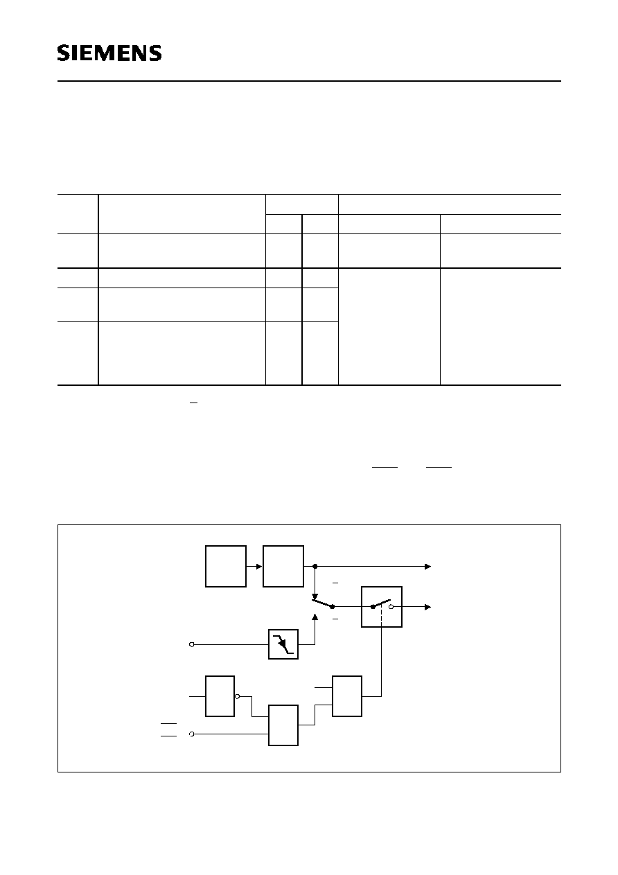
Timer / Counter 0 and 1
Timer/Counter 0 and 1 can be used in four operating modes as listed in table 5 :
In the "timer" function (C/T = `0') the register is incremented every machine cycle. Therefore the
count rate is
f
OSC
/6.
In the "counter" function the register is incremented in response to a 1-to-0 transition at its
corresponding external input pin (P3.4/T0, P3.5/T1). Since it takes two machine cycles to detect a
falling edge the max. count rate is
f
OSC
/12. External inputs INT0 and INT1 (P3.2, P3.3) can be
programmed to function as a gate to facilitate pulse width measurements. Figure 10 illustrates the
input clock logic.
Figure 10
Timer/Counter 0 and 1 Input Clock Logic
Table 5
Timer/Counter 0 and 1 Operating Modes
Mode
Description
TMOD
Input Clock
M1
M0
internal
external (max)
0
8-bit timer/counter with a
divide-by-32 prescaler
0
0
f
OSC
/6x32
f
OSC
/12x32
1
16-bit timer/counter
1
1
f
OSC
/6
f
OSC
/12
2
8-bit timer/counter with
8-bit autoreload
1
0
3
Timer/counter 0 used as one
8-bit timer/counter and one
8-bit timer
Timer 1 stops
1
1
MCS03117
1
&
OSC
C/T = 0
C/T = 1
Control
=1
6
TR1
P3.5/T1
(TMOD)
P3.2/INT0
f
Timer 0/1
Input Clock
OSC
/6
P3.4/T0
TR0
Gate
P3.3/INT1
˜
_
<

Semiconductor Group
26
C541U
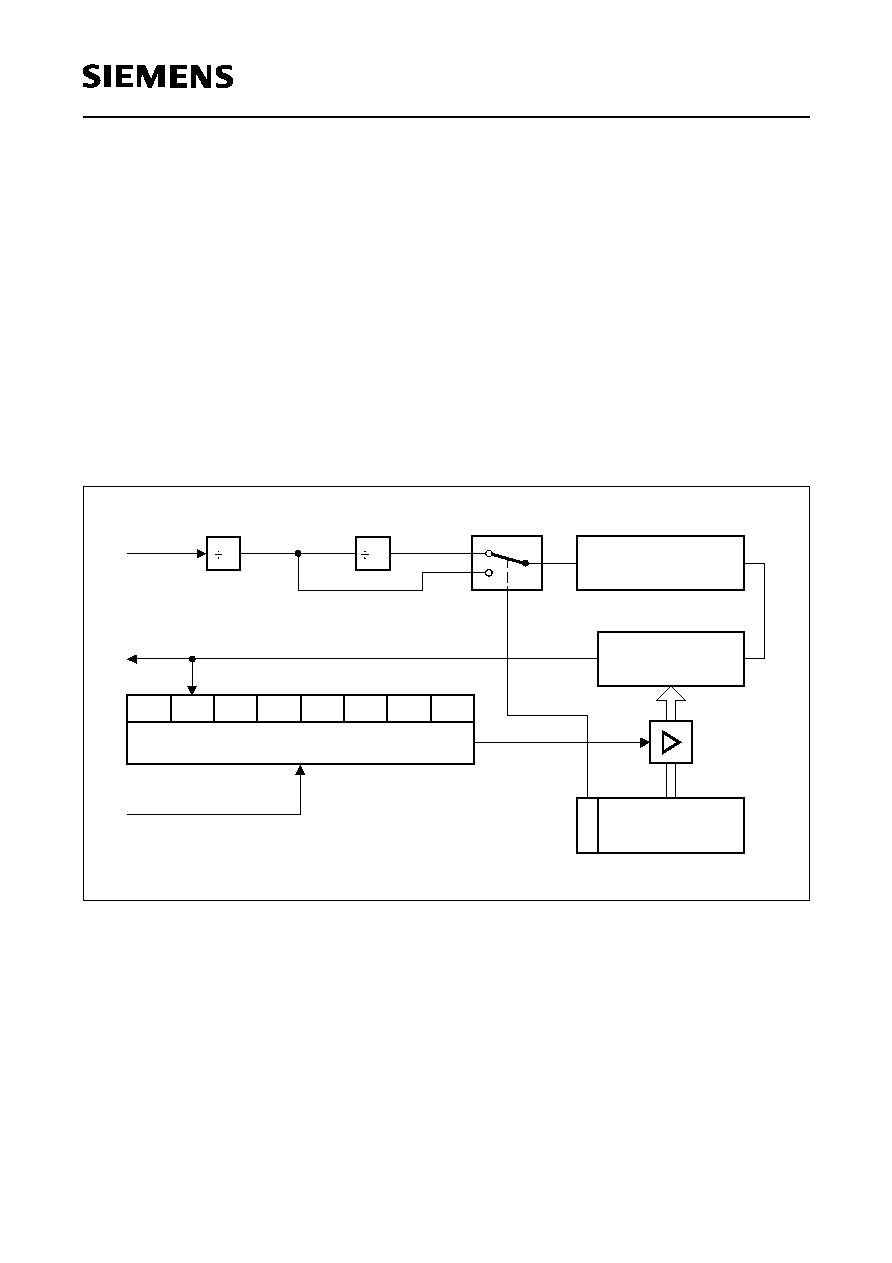
SSC Interface
The C541U microcontroller provides a Synchronous Serial Channel unit, the SSC. This interface is
compatible to the popular SPI serial bus interface. Figure 11 shows the block diagram of the SSC.
The central element of the SSC is an 8-bit shift register. The input and the output of this shift register
are each connected via a control logic to the pin P1.3 / SRI (SSC Receiver In) and P1.4 / STO (SSC
Transmitter Out). This shift register can be written to (SFR STB) and can be read through the
Receive Buffer Register SRB.
Figure 11
SSC Block Diagram
The SSC has implemented a clock control circuit, which can generate the clock via a baud rate
generator in the master mode, or receive the transfer clock in the slave mode. The clock signal is
fully programmable for clock polarity and phase. The pin used for the clock signal is P1.2/ SCLK.
When operating in slave mode, a slave select input is provided which enables the SSC interface
and also will control the transmitter output. The pin used for this is P1.5 / SLS.
The SSC control block is responsible for controlling the different modes and operation of the SSC,
checking the status, and generating the respective status and interrupt signals.
Clock Divider
Clock Selection
Receive Buffer Register
Int. Enable Reg.
Control Register
. . .
f
OSC
Shift Register
STB
SRB
Pin
Control
Logic
Pin
Pin
Pin
Pin
P1.2 / SCLK
P1.3 / SRI
P1.4 / STO
P1.5 / SLS
SCIEN
SSCCON
SCF
Status Register
Control Logic
Interrupt
Internal Bus
MCB03379
Semiconductor Group
27
C541U
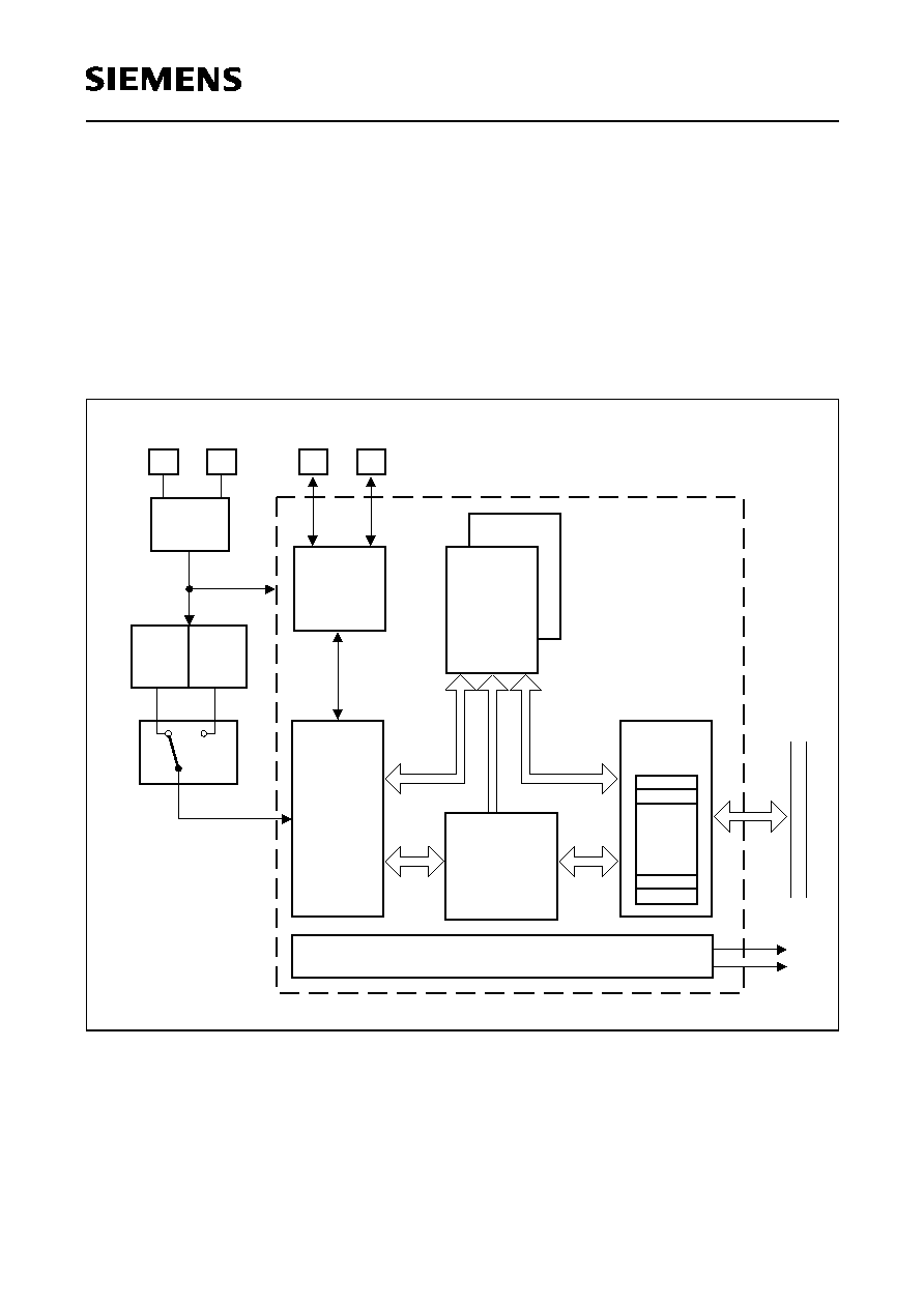
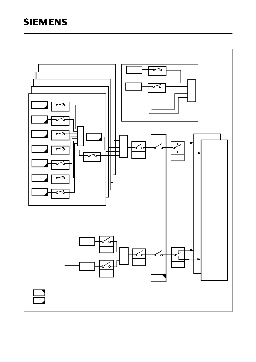
USB Module
The USB module in the C541U handles all transactions between the serial USB bus and the internal
(parallel) bus of the microcontroller. The USB module includes several units which are required to
support data handling with the USB bus : the on-chip USB bus transceiver, the USB memory with
two pages of 128 bytes each, the memory management unit (MMU) for USB and CPU memory
access control, the UDC device core for USB protocol handling, the microcontroller interface with
the USB specific special function registers and the interrupt control logic. A clock generation unit
provides the clock signal for the USB module for full speed and low speed USB operation. Figure
12 shows the block diagram of the functional units of the USB module with their interfaces.
Figure 12
USB Module Block Diagram
MCB03380
Pin
Pin
Pin
Pin
XTAL1
XTAL2
D+
D-
USB Bus
Osc.
12 MHz
(On-chip)
Transceiver
x 4
PLL
2
48 MHz
6 MHz
USB
Page 0
(128 x 8)
F
00
00
Data
Data
Control
USB Memory
Management
MMU
Interrupt Generation
SFR
Addr.
11
Core
Device
USB
MCU
Interface
Module
USB
Internal
Bus
Memory
Page 1
(UDC)
Control
H
H
H
7
7
H
F
Address
Semiconductor Group
28
C541U
USB Full-Speed Registers
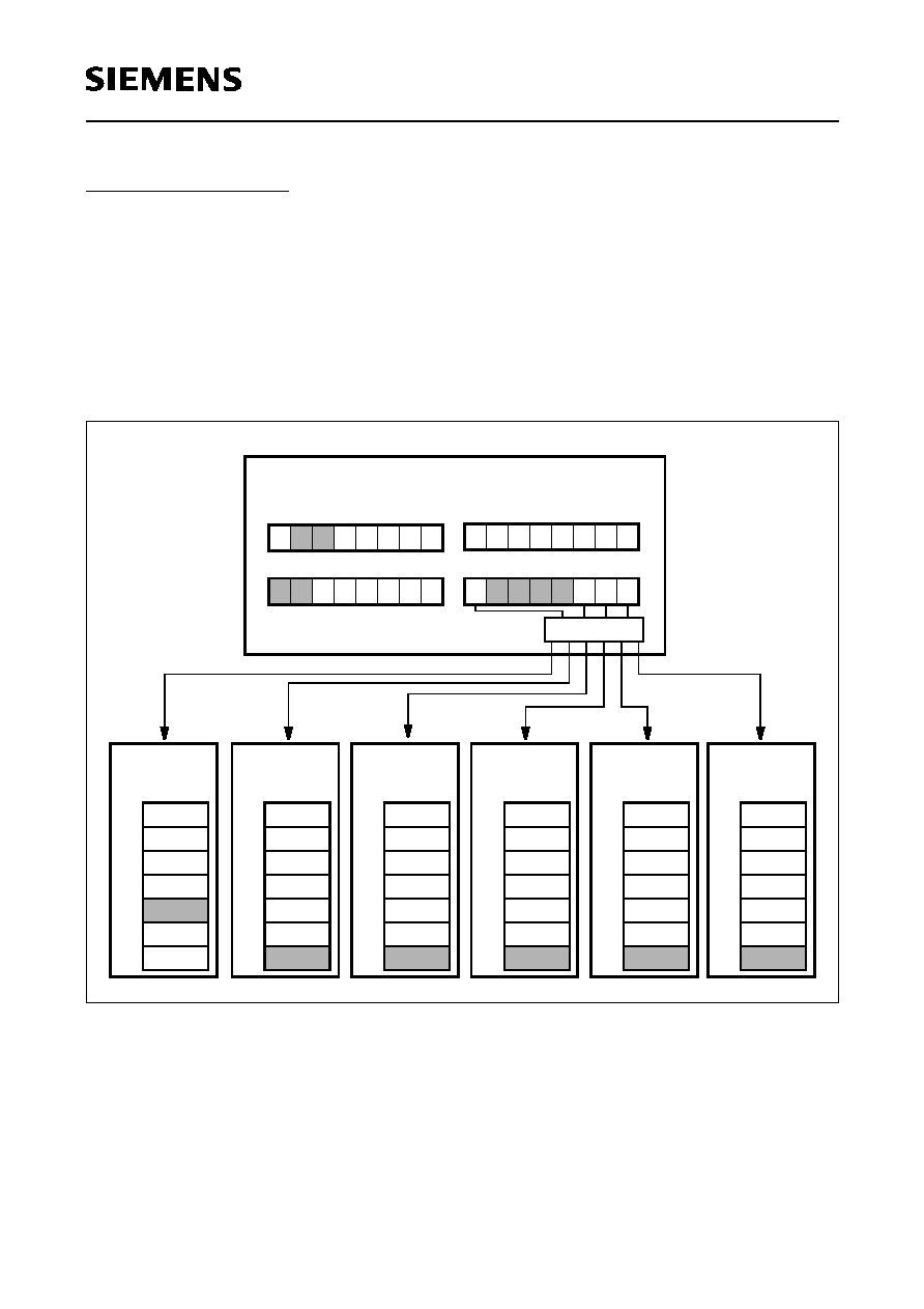
Two different kinds of registers are implemented for full speed operation in the USB module. The
global registers (GEPIR, EPSEL, ADROFF, USBVAL) describe the basic functionality of the
complete USB module and can be accessed via unique SFR addresses. For reduction of the
number of SFR addresses which are needed to control the USB module inside the C541U, device
registers and endpoint registers are mapped into an SFR address block of seven SFR addresses
(C1H to C7H). The endpoint specific functionality of the USB module is controlled via the device
registers DCR, DPWDR, DIER, DIRR and the frame number registers. An endpoint register set is
available for each endpoint (n=0..4) and describes the functionality of the selected endpoint. Figure
13 explains the structure of the USB module registers.
Figure 13
Register Structure of the USB Module
D
Global Registers
EPSEL(D2
H
)
Endpoint 0
Registers
EPBC0
EPBS0
EPIE0
EPIR0
EPBA0
EPLEN0
C1
H
C2
H
C3
H
C4
H
C5
H
C6
H
C7
H
reserved
Endpoint 1
Registers
EPBC1
EPBS1
EPIE1
EPIR1
EPBA1
EPLEN1
C1
H
C2
H
C3
H
C4
H
C5
H
C6
H
C7
H
reserved
Endpoint 2
Registers
EPBC2
EPBS2
EPIE2
EPIR2
EPBA2
EPLEN2
C1
H
C2
H
C3
H
C4
H
C5
H
C6
H
C7
H
reserved
Endpoint 3
Registers
EPBC3
EPBS3
EPIE3
EPIR3
EPBA3
EPLEN3
C1
H
C2
H
C3
H
C4
H
C5
H
C6
H
C7
H
reserved
Endpoint 4
Registers
EPBC4
EPBS4
EPIE4
EPIR4
EPBA4
EPLEN4
C1
H
C2
H
C3
H
C4
H
C5
H
C6
H
C7
H
reserved
Device
Registers
DCR
DIER
DIRR
FNRL
C1
H
C2
H
C3
H
C4
H
C5
H
C6
H
C7
H
reserved
DPWDR
FNRH
.0
.1
.2
.7
USBVAL(D3
H
)
ADROFF(D4
H
)
GEPIR(D6
H
)
.0
.1
.2
.7 .6 .5 .4 .3
.0
.1
.2
.4 .3
.5
.0
.1
.2
.4 .3
0 0
0 0
0 0 0 0
Decoder
Semiconductor Group
29
C541U
Interrupt System
The C541U provides seven interrupt sources with two priority levels. Five interrupts can be
generated by the on-chip peripherals (timer 0, timer 1, SSC interface, and USB module), and two
interrupts may be triggered externally (P3.2/INT0 and P3.3/INT1).
Figure 14 to 16 give a general overview of the interrupt sources and illustrate the request and
control flags which are described in the next sections.
Figure 14
Interrupt Request Sources (Part 1)
EA
ET0
TF0
IEN0.1
TCON.5
000B
H
IEN0.7
Low Priority
MCT03684
Bit addressable
Request flag is cleared by hardware
IP0.1
PT0
High Priority
TCON.7
TF1
ET1
IEN0.3
H
001B
Timer 1
Timer 0
IEN0.0
TCON.1
IE0
0003
EX0
H
Overflow
Overflow
INT0
P3.2 /
IT0
TCON.0
ITCON.0
ITCON.1
>1
ITCON.3
TCON.2
P3.3 /
INT1
IT1
ITCON.2
>1
IEN0.2
TCON.3
IE0
0013
EX1
H
IP0.3
PT1
IP0.0
PX0
PX1
IP0.2
Semiconductor Group
30
C541U
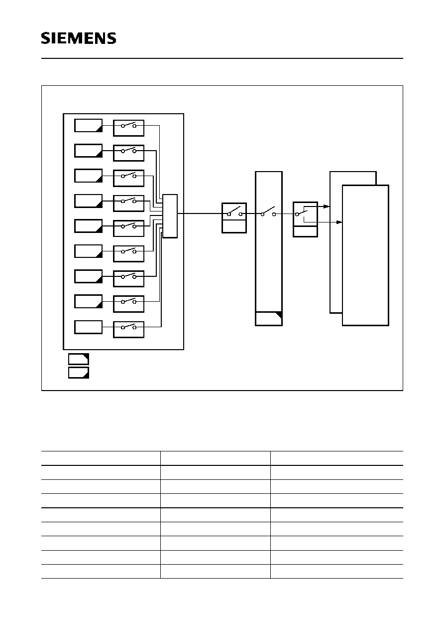
Figure 15
Interrupt Request Sources (Part 2)
Endpoint 4 Interrupts
Endpoint 3 Interrupts
Endpoint 2 Interrupts
Low Priority
High Priority
004B
H
EUEI
IEN1.1
IP1.1
PUEI
IEN0.7
EA
Bit addressable
Request flag is cleared by hardware after the corresponding register has been read.
Endpoint 0 Interrupts
1
ACK0
NACK0
RLE0
DNR0
NOD0
EOD0
AIE0
EPIE0.7
NAIE0
EPIE0.6
RLEIE0
EPIE0.5
DNRIE0
EPIE0.3
NODIE0
EPIE0.2
EODIE0
EPIE0.1
EPIR0.7
EPIR0.6
EPIR0.5
EPIR0.3
EPIR0.2
EPIR0.1
Endpoint 1 Interrupts
1
Endpoint Interrupts
0043
H
ESSC
IEN1.0
SSC
WCEN
TCEN
SCIEN.1
SCIEN.0
1
SCF.0
WCOL
SCF.1
TC
Interrupts
PSSC
IP1.0
GEPIE0
EPBC0.4
EPI0
GEPIR.0
SOD0
SODIE0
EPIE0.0
EPIR0.0
Low Speed Interrupts
1
SUSP
SUSPIE
USBPWD.3
DADD
DADDIE
USBPWD.2
USBPWD.5
USBPWD.4
SETUP packet
OUT packet
USB Reset
Semiconductor Group
31
C541U
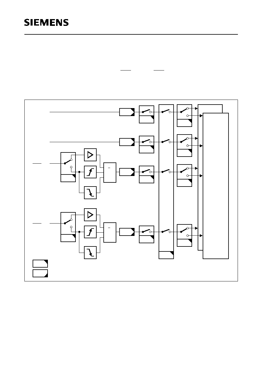
Figure 16
Interrupt Request Sources (Part 3)
Table 6
Interrupt Source and Vectors
Interrupt Source
Interrupt Vector Address
Interrupt Request Flags (SFRs)
External Interrupt 0
0003H
IE0
Timer 0 Overflow
000BH
TF0
External Interrupt 1
0013H
IE1
Timer 1 Overflow
001BH
TF1
SSC Interrupt
0043H
TC, WCOL
USB Endpoint Interrupt
004BH
in SFRs EPIR0-4 and GEPIR
USB Device Interrupt
0053H
in SFRs DIRR and GEPIR
Wake-up from power down
007BH
≠
Low Priority
High Priority
IE0.7
EA
0053
H
IP1.2
PUDI
1
SE0I
DAI
DDI
SBI
SEI
STI
SUI
SE0IE
DIER.7
DAIE
DIER.6
DDIE
DIER.5
SBIE
DIER.4
SEIE
DIER.3
STIE
DIER.2
SUIE
DIER.1
DIRR.7
DIRR.6
DIRR.5
DIRR.4
DIRR.3
DIRR.2
DIRR.1
EUDI
IEN1.2
SOFI
SOFIE
DIER.0
DIRR.0
Device Interrupts
Bit addressable
Request flag is cleared by hardware after the corresponding register has been read.
DRVI
DRVIE
DPWDR.7
GEPIR.7
Semiconductor Group
32
C541U
Fail Save Mechanisms
The C541U offers enhanced fail safe mechanisms, which allow an automatic recovery from
software upset or hardware failure :
≠ a programmable watchdog timer (WDT), with variable time-out period from 256
µ
s up to
approx. 0.55
µ
s at 12 MHz.
≠ an oscillator watchdog (OWD) which monitors the on-chip oscillator and forces the
microcontroller into reset state in case the on-chip oscillator fails; it also provides the clock for
a fast internal reset after power-on.
The watchdog timer in the C541U is a 15-bit timer, which is incremented by a count rate of
f
OSC
/12
or
f
OSC
/192. The system clock of the C541U is divided by two prescalers, a divide-by-two and a
divide-by-16 prescaler which are selected by bit WDTPSEL (WDTREL.7). For programming of the
watchdog timer overflow rate, the upper 7 bit of the watchdog timer can be written. Figure 8-17
shows the block diagram of the watchdog timer unit.
Figure 17
Block Diagram of the Watchdog Timer
The watchdog timer can be started by software (bit SWDT) but it cannot be stopped during active
mode of the C541U. If the software fails to refresh the running watchdog timer an internal reset will
be initiated on watchdog timer overflow. For refreshing of the watchdog timer the content of the SFR
WDTREL is transfered to the upper 7-bit of the watchdog timer. The refresh sequence consists of
two consequtive instructions which set the bits WDT and SWDT each. The reset cause (external
reset or reset caused by the watchdog) can be examined by software (flag WDTS). It must be noted,
however, that the watchdog timer is halted during the idle mode and power down mode of the
processor.
MCB03384
WDCON (CO )
H
OSC
f
-
-
-
-
OWDS WDTS
WDT
SWDT
2
16
14
0
7
8
WDTL
WDTH
/ 6
External HW Reset
Control Logic
6
7
0
WDT Reset-Request
WDTPSEL
WDTREL

Semiconductor Group
33
C541U
Oscillator Watchdog
The oscillator watchdog unit serves for three functions:
≠ Monitoring of the on-chip oscillator's function
The watchdog supervises the on-chip oscillator's frequency; if it is lower than the frequency of
the auxiliary RC oscillator in the watchdog unit, the internal clock is supplied by the RC
oscillator and the device is brought into reset; if the failure condition disappears (i.e. the on-
chip oscillator has a higher frequency than the RC oscillator), the part executes a final reset
phase of typ. 1 ms in order to allow the oscillator to stabilize; then the oscillator watchdog reset
is released and the part starts program execution again.
≠ Fast internal reset after power-on
The oscillator watchdog unit provides a clock supply for the reset before the on-chip oscillator
has started. The oscillator watchdog unit also works identically to the monitoring function.
≠ Control of external wake-up from software power-down mode (description see chapter 9)
When the power-down mode is left by a low level at the INT0 pin or by the USB, the oscillator
watchdog unit assures that the microcontroller resumes operation (execution of the power-
down wake-up interrupt) with the nominal clock rate. In the power-down mode the RC
oscillator and the on-chip oscillator are stopped. Both oscillators are started again when
power-down mode is released. When the on-chip oscillator has a higher frequency than the
RC oscillator, the microcontroller starts operation after a final delay of typ. 1 ms in order to
allow the on-chip oscillator to stabilize.
Semiconductor Group
34
C541U
Figure 18
Functional Block Diagram of the Oscillator Watchdog
Int. Clock
XTAL2
XTAL1
OWDS
MCD03385
WDCON (C0 )
H
3 MHz
f
RC
Delay
1
f
2
f
2
f
1
f
<
Activity on
Start /
Stop
Start /
Stop
Mode Activated
Power - Down
Power-Down Mode
Wake - Up Interrupt
Internal Reset
10
P3.2 / INT0
Control
WS
(PCON1.4)
(PCON1.7)
EWPD
>1
Frequency
Comparator
RC
On-Chip
Oscillator
Logic
Oscillator
Logic
Control
USB Bus

Semiconductor Group
35
C541U
Power Saving Modes
The C541U provides two basic power saving modes, the idle mode and the power down mode.
≠ Idle mode
In the idle mode the main oscillator of the C541U continues to run, but the CPU is gated off
from the clock signal. However, the interrupt system, the SSC, the USB module, and the
timers with the exception of the watchdog timer are further provided with the clock. The CPU
status is preserved in its entirety : the stack pointer, program counter, program status word,
accumulator, and all other registers maintain their data during idle mode. The idle mode can
be terminated by activating any enabled interrupt. or by a hardware reset.
≠ Power down mode
In the power down mode, the RC osciillator and the on-chip oscillator which operates with the
XTAL pins is stopped. Therefore, all functions of the microcontroller are stopped and only the
contents of the on-chip RAM, XRAM and the SFR's are maintained. The power down mode
can be left either by an active reset signal or by a low signal at the P3.2/INT0 pin or any activity
on the USB bus. Using reset to leave power down mode puts the microcontroller with its SFRs
into the reset state. Using the INT0 pin or USB bus for power down mode exit maintains the
state of the SFRs, which has been frozen when power down mode is entered.
In the power down mode of operation,
V
DD
can be reduced to minimize power consumption. It must
be ensured, however, that
V
DD
is not reduced before the power down mode is invoked, and that
V
DD
is restored to its normal operating level, before the power down mode is terminated. Table 7 gives
a general overview of the entry and exit procedures of the power saving modes.
Table 7
Power Saving Modes Overview
Mode
Entering
2-Instruction
Example
Leaving by
Remarks
Idle mode
ORL PCON, #01H
ORL PCON, #20H
Ocurrence of an
interrupt from a
peripheral unit
CPU clock is stopped;
CPU maintains their data;
peripheral units are active (if
enabled) and provided with
clock
Hardware Reset
Power Down Mode
ORL PCON, #02H
ORL PCON, #40H
Hardware Reset
Oscillator is stopped;
contents of on-chip RAM and
SFR's are maintained;
Short low pulse at
pin P3.2/INT0 or
activity on the USB
bus
Semiconductor Group
36
C541U
OTP Memory Operation
The C541U contains a 8k byte one-time programmable (OTP) program memory. With the C541U
fast programming cycles are achieved (1 byte in 100
µ
sec). Also several levels of OTP memory
protection can be selected.
For programming of the device, the C541U must be put into the programming mode. This typically
is done not in-system but in a special programming hardware. In the programming mode the C541U
operates as a slave device similar as an EPROM standalone memory device and must be controlled
with address/data information, control lines, and an external 11.5V programming voltage. Figure 19
shows the pins of the C541U-1E which are required for controlling of the OTP programming mode.
Figure 19
Programming Mode Configuration
Port 0
D0-D7
V
DD
V
SS
C541U
PROG
A0-A7 /
Port 2
EA/V
PP
PMSEL0
PSEL
RESET
PSEN
PMSEL1
PRD
A8-A12
PALE
XTAL1
XTAL2
Semiconductor Group
37
C541U
Pin Configuration in Programming Mode
Figure 20
Pin Configuration of the C541U in Programming Mode (Top View)
6
7
8
9
10
11
12
13
14
15
16
17
5
4
3
2
1
44 43 42 41 40
39
38
37
36
35
34
33
32
31
30
29
18 19 20 21 22 23 24 25 26 27
N.C
.
N.C
.
N.C
.
N.C
.
N.C
.
N.C
.
N.C.
V
DD
V
SS
PMSEL0
N.C.
PMSEL1
PSEL
PRD
PALE
RESET
D3
N.C
.
D2
D1
D0
D4
D5
D6
D7
EA/V
PP
N.C.
PSEN
A7
A6
A5
PROG
28
GN
D
GN
D
X
T
AL2
X
T
AL1
V
SS
V
DD
A0
/
A
8
A1
/
A
9
A2/A10
A3/A11
A4/A12
Programming
Mode
C541U
GND
Semiconductor Group
38
C541U
The following table 8 contains the functional description of all C541U-1E pins which are required for
OTP memory programming.
Table 8
Pin Definitions and Functions in Programming Mode
Symbol
Pin Num-
bers
I/O*) Function
P-LCC-44
RESET
10
I
Reset
This input must be at static "1" (active) level during the whole
programming mode.
PMSEL0
PMSEL1
11
13
I
I
Programming mode selection pins
These pins are used to select the different access modes in
programming mode. PMSEL1,0 must satisfy a setup time to the
rising edge of PALE. When the logic level of PMSEL1,0 is changed,
PALE must be at low level.
PSEL
14
I
Basic programming mode select
This input is used for the basic programming mode selection and
must be switched according figure 10-21.
PRD
15
I
Programming mode read strobe
This input is used for read access control for OTP memory read,
version byte read, and lock bit read operations.
PALE
16
I
Programming mode address latch enable
PALE is used to latch the high address lines. The high address
lines must satisfy a setup and hold time to/from the falling edge of
PALE. PALE must be at low level whenever the logic level of
PMSEL1,0 is changed.
XTAL2
20
O
XTAL2
Output of the inverting oscillator amplifier.
XTAL1
21
I
XTAL1
Input to the oscillator amplifier.
*) I = Input
O = Output
PMSEL
1
PMSEL
0
Access Mode
0
0
Reserved
0
1
Read version bytes
1
0
Program/read lock bits
1
1
Program/read OTP memory byte
Semiconductor Group
39
C541U
A0/A8 -
A7
24 - 31
I
Address lines
P2.0-7 are used as multiplexed address input lines A0-A7 and A8-
A12. A8-A12 must be latched with PALE.
PSEN
32
I
Program store enable
This input must be at static "0" level during the whole programming
mode.
PROG
33
I
Programming mode write strobe
This input is used in programming mode as a write strobe for OTP
memory program and lock bit write operations During basic
programming mode selection a low level must be applied to PROG.
EA/V
PP
35
I
External Access / Programming voltage
This pin must be at 11.5 V (V
PP
) voltage level during programming
of an OTP memory byte or lock bit. During an OTP memory read
operation this pin must be at high level (V
IH
). This pin is also used
for basic programming mode selection. At basic programming
mode selection a low level must be applied to EA/V
PP
.
D0 - 7
43 - 36
I/O
Data lines 0-7
During programming mode, data bytes are read or written from or
to the C541U via the bidirectional D0-7 lines which are located at
port 0.
V
SS
9, 22
≠
Circuit ground potential
must be applied to these pins in programming mode.
V
DD
8, 23
≠
Power supply terminal
must be applied to these pins in programming mode.
N.C.
1 - 7, 12,,
34, 44
≠
Not Connected
These pins should not be connected in programming mode.
GND
17 - 19
I
Ground pins
In programming mode these pins must be connected to
V
IL
level.
*) I = Input
O = Output
Table 8
Pin Definitions and Functions in Programming Mode (cont'd)
Symbol
Pin Num-
bers
I/O*) Function
P-LCC-44
Semiconductor Group
40
C541U
Basic Programming Mode Selection
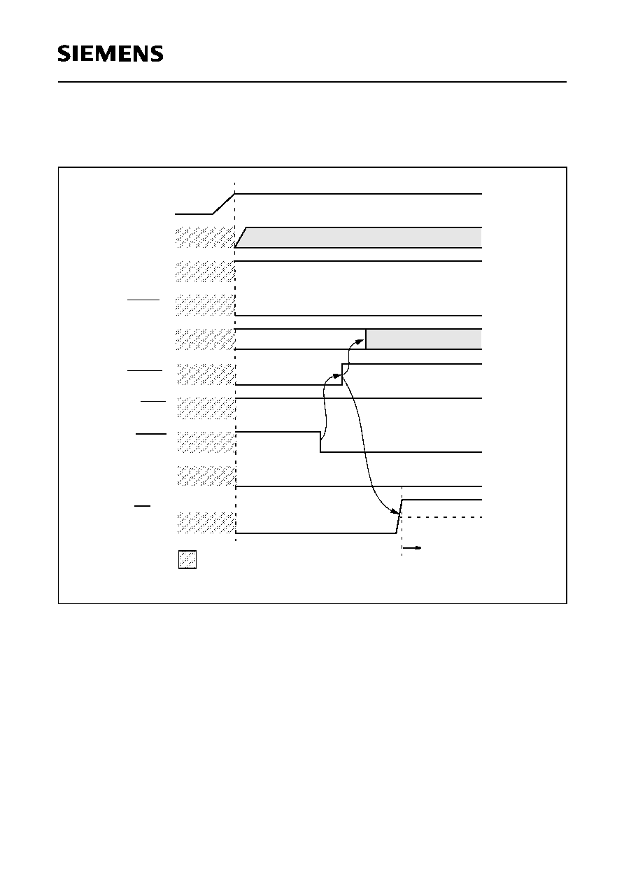
The basic programming mode selection scheme is shown in figure 21.
Figure 21
Basic Programming Mode Selection
RESET
PSEN
PROG
EA/V
PP
"1"
"0"
PSEL
"0"
V
DD
Clock
(XTAL1/XTAL2)
5V
stable
PRD
PALE
"1"
"0"
Ready for access
mode selection
During this period signals
are not actively driven
0V
V
IH1
V
PP
PMSEL1,0
0,1
Semiconductor Group
41
C541U
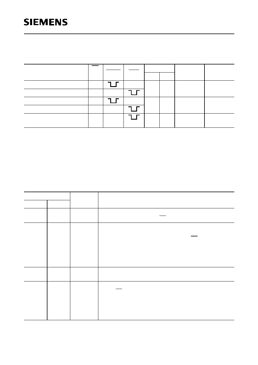
Lock Bits Programming / Read
The C541U has two programmable lock bits which, when programmed according tabie 10, provide
four levels of protection for the on-chip OTP code memory. The state of the lock bits can also be
read.
Table 9
Access Modes Selection
Access Mode
EA/
V
PP
PROG
PRD
PMSEL
Address
(Port 2)
Data
(Port 0)
1
0
Program OTP memory byte
V
PP
H
H
H
A0-7
A8-15
D0-7
Read OTP memory byte
V
IH
H
Program OTP lock bits
V
PP
H
H
L
≠
D1,D0 see
table 10
Read OTP lock bits
V
IH
H
Read OTP version byte
V
IH
H
L
H
Byte addr.
of sign. byte
D0-7
Table 10
Lock Bit Protection Types
Lock Bits at D1,D0
Protection
Level
Protection Type
D1
D0
1
1
Level 0
The OTP lock feature is disabled. During normal operation of
the C541U, the state of the EA pin is not latched on reset.
1
0
Level 1
During normal operation of the C541U, MOVC instructions
executed from external program memory are disabled from
fetching code bytes from internal memory. EA is sampled and
latched on reset. An OTP memory read operation is only
possible using the OTP verification mode for protection level 1.
Further programming of the OTP memory is disabled
(reprogramming security).
0
1
Level 2
Same as level 1, but also OTP memory read operation using
OTP verification mode is disabled.
0
0
Level 3
Same as level 2; but additionally external code execution by
setting EA=low during normal operation of the C541U is no
more possible.
External code execution, which is initiated by an internal
program (e.g. by an internal jump instruction above the ROM
boundary), is still possible.

Semiconductor Group
42
C541U
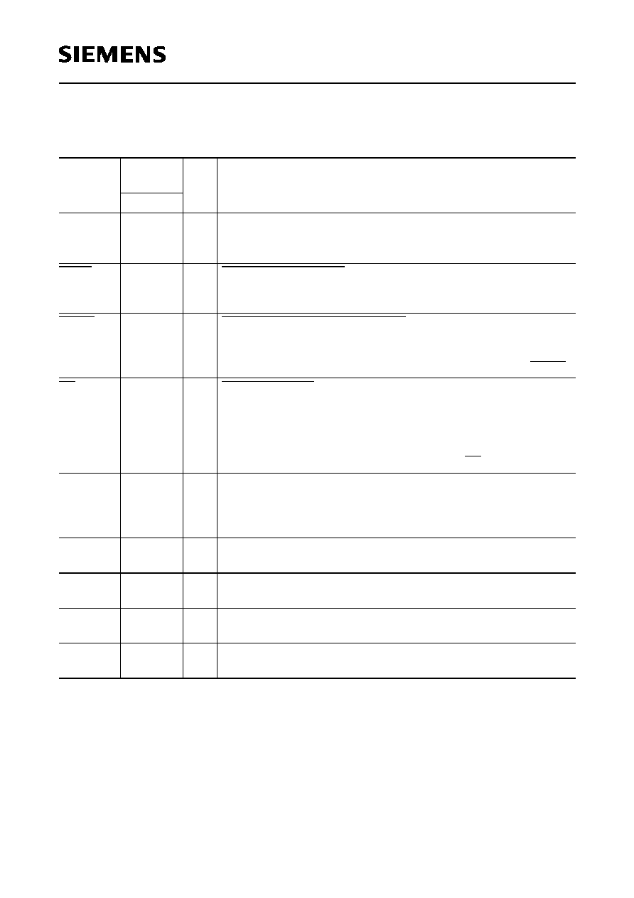
Absolute Maximum Ratings
Note: Stresses above those listed under "Absolute Maximum Ratings" may cause permanent
damage of the device. This is a stress rating only and functional operation of the device at
these or any other conditions above those indicated in the operational sections of this
specification is not implied. Exposure to absolute maximum rating conditions for longer
periods may affect device reliability. During absolute maximum rating overload conditions
(
V
IN
>
V
DD
or
V
IN
<
V
SS
) the voltage on
V
DD
pins with respect to ground (
V
SS
) must not exceed
the values defined by the absolute maximum ratings.
Operating Conditions
Parameter
Symbol
Limit Values
Unit
Notes
min.
max.
Storage temperature
T
ST
≠ 65
150
∞C
≠
Voltage on
V
DD
pins with respect
to ground (
V
SS
)
V
DD
≠0.5
6.5
V
≠
Voltage on any pin with respect
to ground (
V
SS
)
V
IN
≠0.5
V
DD
+
0.5
V
≠
Input current on any pin during
overload condition
≠
10
10
mA
≠
Absolute sum of all input
currents during overload
condition
≠
| 100 |
mA
≠
Power dissipation
P
DISS
≠
TBD
W
≠
Parameter
Symbol
Limit Values
Unit
Notes
min.
max.
Supply voltage
V
DD
4.25
5.5
V
≠
Ground voltage
V
SS
0
V
≠
Ambient temperature
T
A
0
70
∞C
≠
CPU clock
f
CPU
2
12
MHz ≠

Semiconductor Group
43
C541U
DC Characteristics
(Operating Conditions apply)
Notes see next page
Parameter
Symbol
Limit Values
Unit
Test Condition
min.
max.
Input low voltage (except EA,
RESET)
V
IL
≠ 0.5
0.2
V
DD
≠
0.1
V
≠
Input low voltage (EA)
V
IL1
≠ 0.5
0.2
V
DD
≠
0.3
V
≠
Input low voltage (RESET)
V
IL2
≠ 0.5
0.2
V
DD
+
0.1
V
≠
Input high voltage (except XTAL1,
RESET and EA)
V
IH
0.2
V
DD
+
0.9
V
DD
+ 0.5
V
≠
Input high voltage to XTAL1
V
IH1
0.7
V
DD
V
DD
+ 0.5
V
≠
Input high voltage to RESET and
EA
V
IH2
0.6
V
DD
V
DD
+ 0.5
V
≠
Output low voltage
Ports 1, 2, 3
P1.0, P1.1, P3.0
V
OL
≠
≠
0.45
0.45
V
V
I
OL
= 1.6 mA
1)
I
OL
= 10 mA
1)
Output low voltage (ALE, PSEN)
V
OL1
≠
0.45
V
I
OL
= 3.2 mA
1)
Output low voltage (Port 0)
V
OL2
≠
0.6
V
I
OL
= 3.2 mA
1)
Output high voltage (ports 1, 2, 3)
V
OH
2.4
0.9
V
DD
≠
≠
V
I
OH
= ≠ 80
µ
A,
I
OH
= ≠ 10
µ
A
Output high voltage (port 0 in
external bus mode, ALE, PSEN)
V
OH2
2.4
0.9
V
DD
≠
≠
V
I
OH
= ≠ 800
µ
A
I
OH
= ≠ 80
µ
A
2)
Logic 0 input current (ports 1, 2, 3)
I
IL
≠ 10
≠ 60
µ
A
V
IN
= 0.45 V
Logical 1-to-0 transition current
(ports 1, 2, 3)
I
TL
≠ 65
≠ 650
µ
A
V
IN
= 2 V
Input leakage current (port 0, EA)
I
LI
≠
±
1
µ
A
0.45 <
V
IN
<
V
DD
Pin capacitance
C
IO
≠
10
pF
f
c
= 1 MHz,
T
A
= 25
∞
C
7)
Overload current
I
OV
≠
±
5
mA
6) 7)
Programming voltage
V
PP
10.9
12.1
V
11.5 V ± 5%
Semiconductor Group
44
C541U
Power Supply Current
Notes :
1) Capacitive loading on ports 0 and 2 may cause spurious noise pulses to be superimposed on the
V
OL
of ALE
and port 3. The noise is due to external bus capacitance discharging into the port 0 and port 2 pins when these
pins make 1-to-0 transitions during bus operation. In the worst case (capacitive loading > 100 pF), the noise
pulse on ALE line may exceed 0.8 V. In such cases it may be desirable to qualify ALE with a schmitt-trigger,
or use an address latch with a schmitt-trigger strobe input.
2) Capacitive loading on ports 0 and 2 may cause the
V
OH
on ALE and PSEN to momentarily fall below the 0.9
V
DD
specification when the address lines are stabilizing.
3)
I
PD
(power-down mode) is measured under following conditions:
EA = Port 0 =
V
DD
; XTAL2 = N.C.; XTAL1 =
V
SS
; RESET =
V
SS
; all other pins are disconnected.
the USB transceiver is switched off;
4)
I
DD
(active mode) is measured with:
XTAL1 driven with
t
CLCH
,
t
CHCL
= 5 ns ,
V
IL
=
V
SS
+ 0.5 V,
V
IH
=
V
DD
≠ 0.5 V; XTAL2 = N.C.;
EA = RESET = Port 0 = Port 1 =
V
DD
; all other pins are disconnected.
I
DD
would be slightly higher if a crystal oscillator is used (appr. 1 mA).
5)
I
DD
(idle mode) is measured with all output pins disconnected and with all peripherals disabled;
XTAL1 driven with
t
CLCH
,
t
CHCL
= 5 ns,
V
IL
=
V
SS
+ 0.5 V,
V
IH
=
V
DD
≠ 0.5 V; XTAL2 = N.C.;
EA = RESET =
V
ss
; Port 0 =
V
DD
; all other pins are disconnected;
6) Overload conditions under operating conditions occur if the voltage on the respective pin exceeds the specified
operating range (i.e.
V
OV
>
V
DD
+ 0.5 V or
V
OV
<
V
SS
- 0.5 V). The absolute sum of input currents on all port
pins may not exceed 50 mA. The supply voltage
V
DD
and
V
SS
must remain within the specified limits.
7) Not 100% tested, guaranteed by design characterization.
8) The typical
I
DD
values are periodically measured at
T
A
= +25 ∞C but not 100% tested.
9) The maximum
I
DD
values are measured under worst case conditions (
T
A
= 0 ∞C and
V
DD
= 5.5 V)
Parameter
Symbol
Limit Values
Unit Test Condition
typ.
8)
max.
9)
Active mode
12 MHz
I
DD
25
30
mA
4)
Idle mode
12 MHz
I
DD
15
20
mA
5)
Power-down mode
I
PD
5
50
µ
A
V
DD
= 2
...
5.5 V
3)
Semiconductor Group
45
C541U
AC Characteristics
(Operating Conditions apply)
(
C
L
for port 0, ALE and PSEN outputs = 100 pF;
C
L
for all other outputs = 80 pF)
Program Memory Characteristics
*)
Interfacing the C541U to devices with float times up to 28 ns is permissible. This limited bus contention will not
cause any damage to port 0 drivers.
**)
For correct function of the USB module the C541U must operate with 12 MHz external clock. The
microcontroller (except the USB module) operates down to 2 MHz.
Parameter
Symbol
Limit Values
Unit
10-MHz clock
Duty Cycle
0.4 to 0.6
Variable Clock
1/CLP = 2 MHz to
12 MHz **)
min.
max.
min.
max.
ALE pulse width
t
LHLL
43
≠
CLP - 40
≠
ns
Address setup to ALE
t
AVLL
13
≠
TCL
Hmin
-20 ≠
ns
Address hold after ALE
t
LLAX
13
≠
TCL
Hmin
-20 ≠
ns
ALE to valid instruction in
t
LLIV
≠
80
≠
2 CLP - 87
ns
ALE to PSEN
t
LLPL
13
≠
TCL
Lmin
-20
≠
ns
PSEN pulse width
t
PLPH
86
≠
CLP+
TCL
Hmin
-30
≠
ns
PSEN to valid instruction in
t
PLIV
≠
51
≠
CLP+
TCL
Hmin
- 65
ns
Input instruction hold after PSEN
t
PXIX
0
≠
0
≠
ns
Input instruction float after PSEN
t
PXIZ
*)
≠
23
≠
TCL
Lmin
-10
ns
Address valid after PSEN
t
PXAV
*)
28
≠
TCL
Lmin
- 5
≠
ns
Address to valid instruction in
t
AVIV
≠
140
≠
2 CLP +
TCL
Hmin
-60
ns
Address float to PSEN
t
AZPL
0
0
≠
ns

Semiconductor Group
46
C541U
AC Characteristics (cont'd)
External Data Memory Characteristics
Parameter
Symbol
Limit Values
Unit
10-MHz
clock
Duty Cycle
0.4 to 0.6
Variable Clock
1/CLP= 2 MHz to 12 MHz
min.
max.
min.
max.
RD pulse width
t
RLRH
180
≠
3 CLP - 70
≠
ns
WR pulse width
t
WLWH
180
≠
3 CLP - 70
≠
ns
Address hold after ALE
t
LLAX2
56
≠
CLP
- 27
≠
ns
RD to valid data in
t
RLDV
≠
110
≠
2 CLP+
TCL
Hmin
- 90
ns
Data hold after RD
t
RHDX
0
0
≠
ns
Data float after RD
t
RHDZ
≠
63
≠
CLP - 20
ns
ALE to valid data in
t
LLDV
≠
200
≠
4 CLP - 133
ns
Address to valid data in
t
AVDV
≠
211
≠
4 CLP +
TCL
Hmin
-155
ns
ALE to WR or RD
t
LLWL
66
166
CLP +
TCL
Lmin
- 50
CLP+
TCL
Lmin
+ 50
ns
Address valid to WR
t
AVWL
70
≠
2 CLP - 97
≠
ns
WR or RD high to ALE high
t
WHLH
8
58
TCL
Hmin
- 25
TCL
Hmin
+ 25
ns
Data valid to WR transition
t
QVWX
8
≠
TCL
Lmin
- 25
≠
ns
Data setup before WR
t
QVWH
163
≠
3 CLP +
TCL
Lmin
- 120
≠
ns
Data hold after WR
t
WHQX
8
≠
TCL
Hmin
- 25
≠
ns
Address float after RD
t
RLAZ
≠
0
≠
0
ns
Semiconductor Group
47
C541U
AC Characteristics (cont'd)
External Clock Drive Characteristics
Parameter
Symbol
CPU Clock = 12 MHz
Duty cycle 0.4 to 0.6
Variable CPU Clock
1/CLP = 2 to 12 MHz
Unit
min.
max.
min.
max.
Oscillator period
CLP
83.3
83.3
83.3
500
ns
High time
TCL
H
33
≠
33
CLP-TCL
L
ns
Low time
TCL
L
33
≠
33
CLP-TCL
H
ns
Rise time
t
R
≠
12
≠
12
ns
Fall time
t
F
≠
12
≠
12
ns
Oscillator duty cycle
DC
0.4
0.6
33 / CLP
1 - 33 / CLP
≠
Clock cycle
TCL
33
50
CLP * DC
min
CLP * DC
max
ns
SSC Interface Characteristics
Parameter
Symbol
Limit Values
Unit
min.
max.
Clock Cycle Time : Master Mode
Slave Mode
t
SCLK
t
SCLK
667
667
≠
≠
ns
ns
Clock high time
t
SCH
300
≠
ns
Clock low time
t
SCL
300
≠
ns
Data output delay
t
D
≠
100
ns
Data output hold
t
HO
0
≠
ns
Data input setup
t
S
100
≠
ns
Data input hold
t
HI
50
≠
ns
TC bit set delay
t
DTC
≠
8 CLP
ns
SLS low to first SCLK clock edge
t
SC
2
t
CLCL
≠
ns
Last SCLK clock edge to SLS high
t
CS
t
CLCL
≠
ns
SLS low to STO active
t
TS
0
100
ns
SLS high to STO tristate
t
ST
≠
100
ns
Data output delay (already defined)
t
D
≠
100
ns
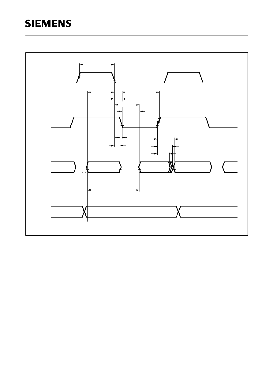
Semiconductor Group
48
C541U
Figure 22
Program Memory Read Cycle
MCT00096
ALE
PSEN
Port 2
LHLL
t
A8 - A15
A8 - A15
A0 - A7
Instr.IN
A0 - A7
Port 0
t
AVLL
PLPH
t
t
LLPL
t
LLIV
t
PLIV
t
AZPL
t
LLAX
t
PXIZ
t
PXIX
t
AVIV
t
PXAV
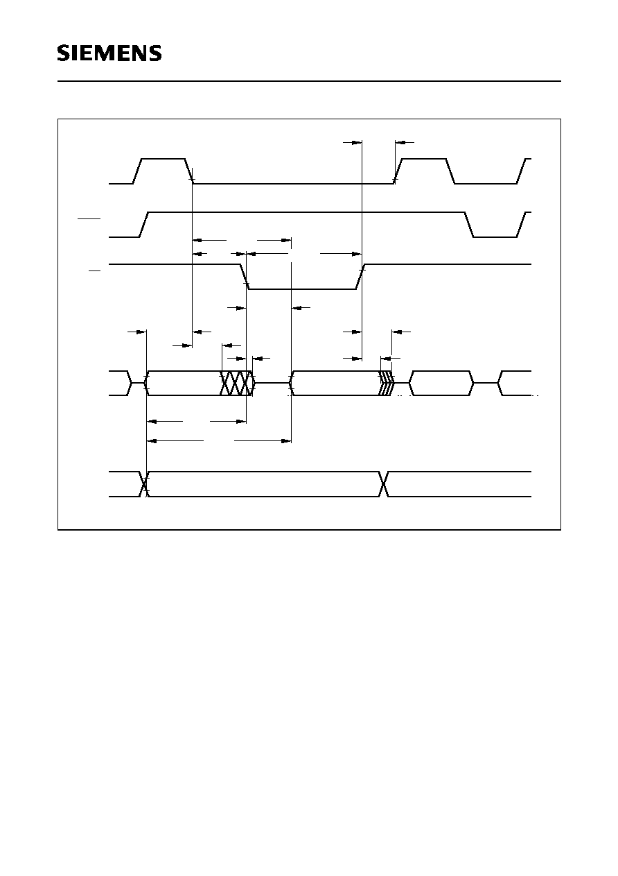
Semiconductor Group
49
C541U
Figure 23
Data Memory Read Cycle
MCT00097
ALE
PSEN
Port 2
WHLH
t
Port 0
RD
t
LLDV
t
RLRH
t
LLWL
t
RLDV
t
AVLL
t
LLAX2
t
RLAZ
t
AVWL
t
AVDV
t
RHDX
t
RHDZ
A0 - A7 from
Ri or DPL
from PCL
A0 - A7
Instr.
IN
Data IN
A8 - A15 from PCH
P2.0 - P2.7 or A8 - A15 from DPH
Semiconductor Group
50
C541U
Figure 24
Data Memory Write Cycle
Figure 25
External Clock Drive on XTAL1
MCT00098
ALE
PSEN
Port 2
WHLH
t
Port 0
WR
t
WLWH
t
LLWL
t
QVWX
t
AVLL
t
LLAX2
t
QVWH
t
AVWL
t
WHQX
A0 - A7 from
Ri or DPL
from PCL
A0 - A7
Instr.IN
Data OUT
A8 - A15 from PCH
P2.0 - P2.7 or A8 - A15 from DPH
TCL
H
TCL
L
CLP
t
R
t
F
0.2 V
CC
0.7
CC
V
- 0.1
MCT03310
XTAL1
V
DD
V
DD
Semiconductor Group
51
C541U
Figure 26
SSC Master Mode Timing
Notes :
Shown is the data/clock relationship for CPOL=CPHA=1. The timing diagram is valid for the other
cases accordingly.
In the case of slave mode and CPHA=0, the output delay for the MSB applies to the falling edge
of SLS (if transmitter is enabled).
In the case of master mode and CPHA=0, the MSB becomes valid after the data has been written
into the shift register, i.e. at least one half SCLK clock cycle before the first clock transition.
Semiconductor Group
52
C541U
Figure 27
SSC Slave Mode Timing
t
SCLK
SCH
t
SCL
t
SCLK (CPOL = 1)
SCLK (CPOL = 0)
SLS
STO (CPHA = 0)
STO (CPHA = 1)
t
TS
t
D
t
D
t
D
D
t
t
D
t
ST
CS
t
SC
t
DOUT 7
DOUT 0
DOUT 7
DOUT 1
DOUT 0
MCT03390
Semiconductor Group
53
C541U
AC Characteristics of Programming Mode
V
DD
= 5 V
±
10 %;
V
PP
= 11.5 V
±
5 %;
T
A
= 25 ∞C
±
10 ∞C
Parameter
Symbol
Limit Values
Unit
min.
max.
ALE pulse width
t
PAW
35
≠
ns
PMSEL setup to ALE rising edge
t
PMS
10
≠
Address setup to ALE, PROG, or PRD falling
edge
t
PAS
10
≠
ns
Address hold after ALE, PROG, or PRD
falling edge
t
PAH
10
≠
ns
Address, data setup to PROG or PRD
t
PCS
100
≠
ns
Address, data hold after PROG or PRD
t
PCH
0
≠
ns
PMSEL setup to PROG or PRD
t
PMS
10
≠
ns
PMSEL hold after PROG or PRD
t
PMH
10
≠
ns
PROG pulse width
t
PWW
100
≠
µ
s
PRD pulse width
t
PRW
100
≠
ns
Address to valid data out
t
PAD
≠
75
ns
PRD to valid data out
t
PRD
≠
20
ns
Data hold after PRD
t
PDH
0
≠
ns
Data float after PRD
t
PDF
≠
20
ns
PROG high between two consecutive PROG
low pulses
t
PWH1
1
≠
µ
s
PRD high between two consecutive PRD low
pulses
t
PWH2
100
ns
XTAL clock period
t
CLKP
83.3
500
ns
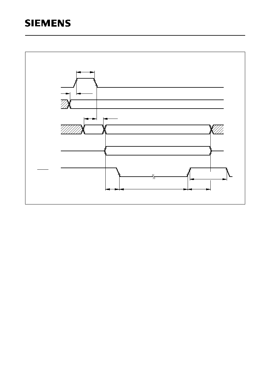
Semiconductor Group
54
C541U
Figure 28
Programming Code Byte - Write Cycle Timing
t
PAW
t
PMS
PAH
t
PAS
t
A8-A13
A0-A7
D0-D7
PCS
t
PWW
t
PCH
t
t
PWH
MCT03369
H, H
PALE
PMSEL1,0
Port 2
Port 0
PROG
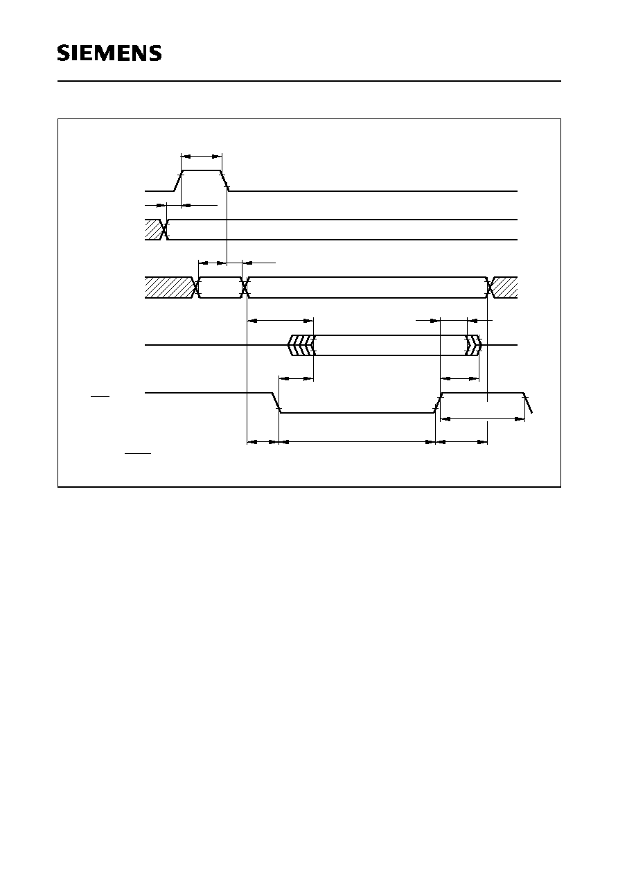
Semiconductor Group
55
C541U
Figure 29
Verify Code Byte - Read Cycle Timing
t
PAW
t
PMS
PAH
t
PAS
t
A8-13
A0-7
PAD
t
D0-7
t
PDH
t
PDF
PRD
t
PCS
t
PRW
t
PCH
t
t
PWH
MCT03392
H, H
PALE
PMSEL1,0
Port 2
Port 0
PRD
Notes: PROG must be high during a programming read cycle.
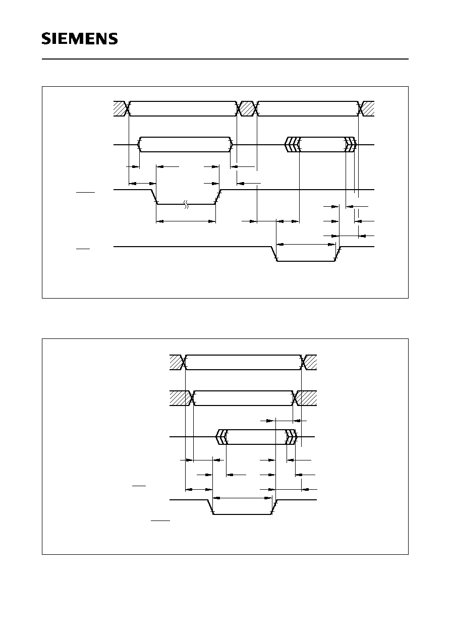
Semiconductor Group
56
C541U
Figure 30
Lock Bit Access Timing
Figure 31
Version Byte Read Timing
H, L
H, L
D0, D1
D0, D1
t
PCS
PMS
t
PMH
t
t
PCH
PWW
t
PMS
t
PRD
t
t
PDH
PDF
t
PMH
t
PRW
t
MCT03393
PMSEL1,0
Port 0
PROG
PRD
PALE should be low during a lock bit read / write cycle.
Note:
e. g. FD
D0-7
t
PCS
PMS
t
t
PDH
PDF
t
PMH
t
MCT03394
Port 2
Port 0
PRD
PMSEL1,0
L, H
H
PRW
t
PRD
t
PCH
t
PROG must be high during a programming read cycle.
Note:
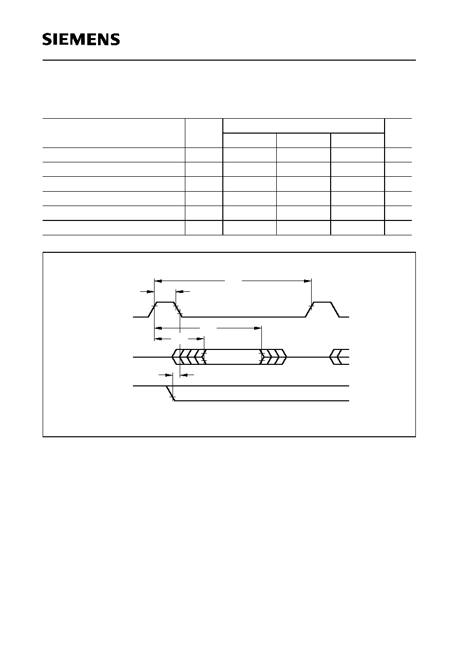
Semiconductor Group
57
C541U
OTP Verification Characteristics
OTP Verification Mode for Protection Level 1
Figure 32
OTP Verification Mode for Protection Level 1
Parameter
Symbol
Limit Values
Unit
min.
typ
max.
ALE pulse width
t
AWD
≠
2
t
CLCL
≠
ns
ALE period
t
ACY
≠
12
t
CLCL
≠
ns
Data valid after ALE
t
DVA
≠
≠
4
t
CLCL
ns
Data stable after ALE
t
DSA
8
t
CLCL
≠
≠
ns
P3.5 setup to ALE low
t
AS
≠
t
CLCL
≠
ns
Oscillator frequency
1/
t
CLCL
4
≠
6
MHz
MCT02613
t
ACY
t
AWD
t
DSA
DVA
t
t
AS
Data Valid
ALE
Port 0
P3.5
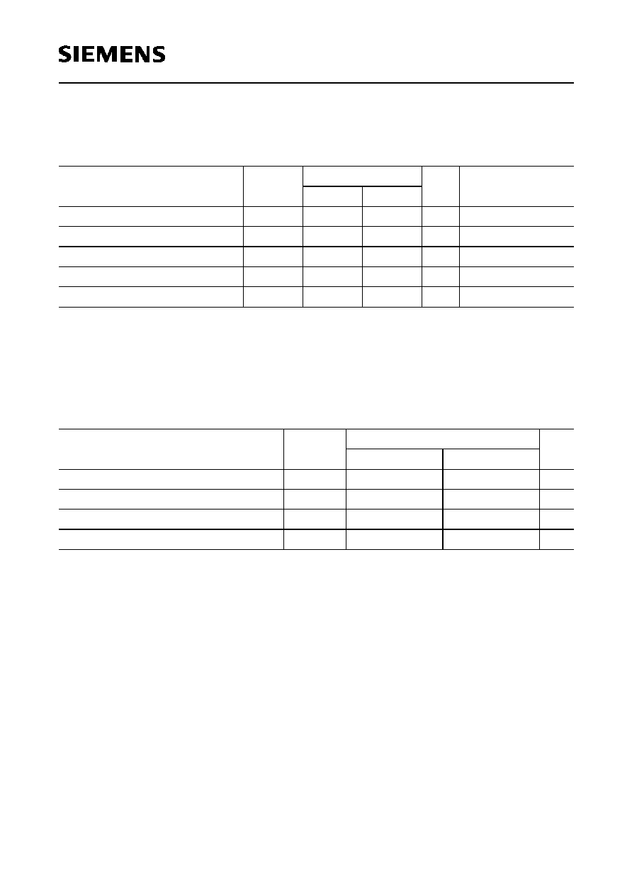
Semiconductor Group
58
C541U
USB Transceiver Characteristics
(Operating Conditions apply)
Notes :
1) This value includes an external resistor of 30
± 1% (see "Load for D+/D-" diagram for testing details)
2) The crossover point is in the range of 1.3V to 2.0V for the high speed mode with a 50pF capacitance. In the
low-speed mode with a 100pF or greater capacitance, the crossover point is in the range of 1.3V to 2.0V.
Parameter
Symbol
Limit Values
Unit
Test Condition
min.
max.
Output impedance (high state)
R
DH
28
43
1)
Output impedance (low state)
R
DL
28
51
Input leakage current
I
I
≠
± 5
µ
A
V
IN
=
V
SS
or
V
DD
Tristate output off-state current
I
OZ
≠
± 10
µ
A
V
OUT
=
V
SS
or
V
DD
1)
Crossover point
V
CR
1.3
2.0
V
2)
Parameter
Symbol
Limit Values
Unit
min.
max.
High speed mode rise time
t
FR
4
20
ns
High speed mode fall time
t
FF
4
20
ns
Low speed mode rise time
t
LR
75
300
ns
Low speed mode fall time
t
LF
75
300
ns
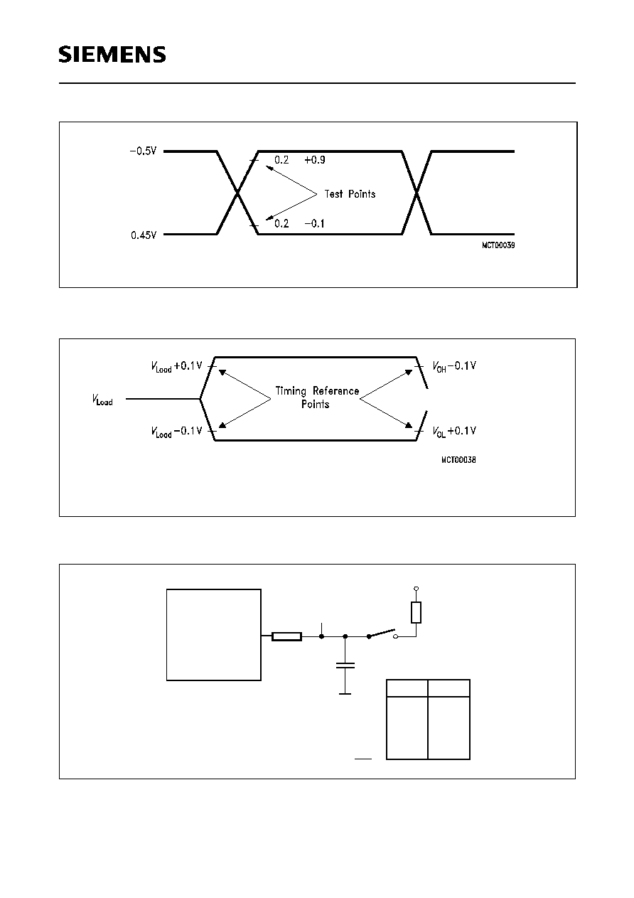
Semiconductor Group
59
C541U
Figure 33
AC Testing: Input, Output Waveforms
Figure 34
AC Testing : Float Waveforms
Figure 35
Load for D+/D-
V
DD
V
DD
V
DD
AC Inputs during testing are driven at
V
DD
- 0.5 V for a logic '1' and 0.45 V for a logic '0'.
Timing measurements are made at
V
IHmin
for a logic '1' and
V
ILmax
for a logic '0'.
For timing purposes a port pin is no longer floating when a 100 mV change from load voltage
occurs and begins to float when a 100 mV change from the loaded
V
OH
/
V
OL
level occurs.
I
OL
/
I
OH
±
20 mA
Test Point
30 k
15 k
D.U.T
C
L
2.8 V
1.5 k
*)
S1
MCS03425
C
L
L
C
L
C
= 50 pF, full speed
= 50 pF, low speed (min. timing)
= 350 pF, low speed (max. timing)
*) 1.5 k
on D- (low speed) or D+ (full speed) only
Test
S1
D- / LS
D+ / LS
D- / FS
D+ / FS
Open
Open
Close
Close
3.3V
27
D.U.T.
D+/D-
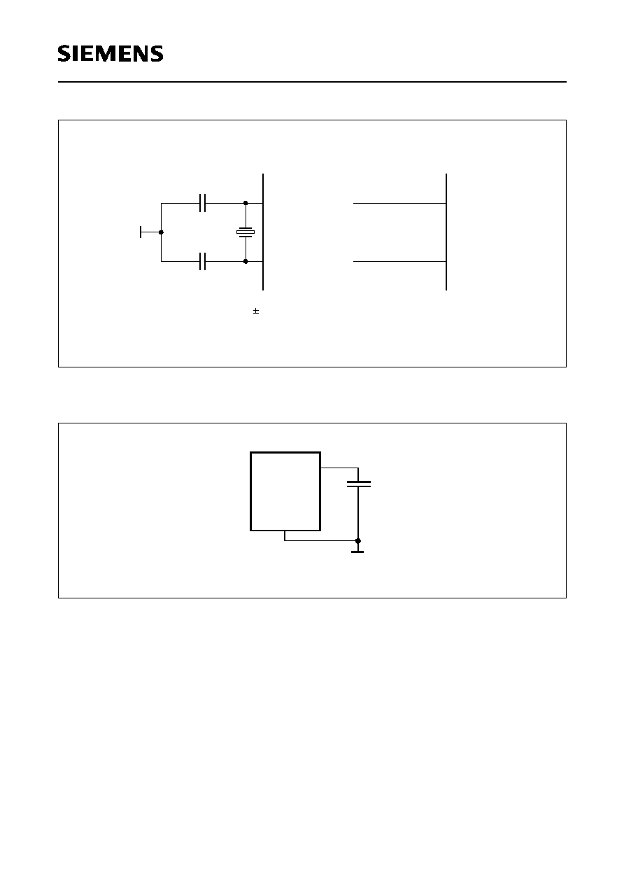
Semiconductor Group
60
C541U
Figure 36
Recommended Oscillator Circuits for Crystal Oscillator
Figure 37
Recommended External Capacitor for On-Chip USB Transceiver
MCS03426
C
C
2 - 12
MHz
XTAL2
XTAL1
XTAL1
XTAL2
N.C.
External Oscillator
Signal
Crystal Oscillator Mode
Driving from External Source
Crystal Mode: C = 20 pF 10 pF
(Incl. Stray Capacitance)
C541U
2
V
SS
C = 6.8nF
9
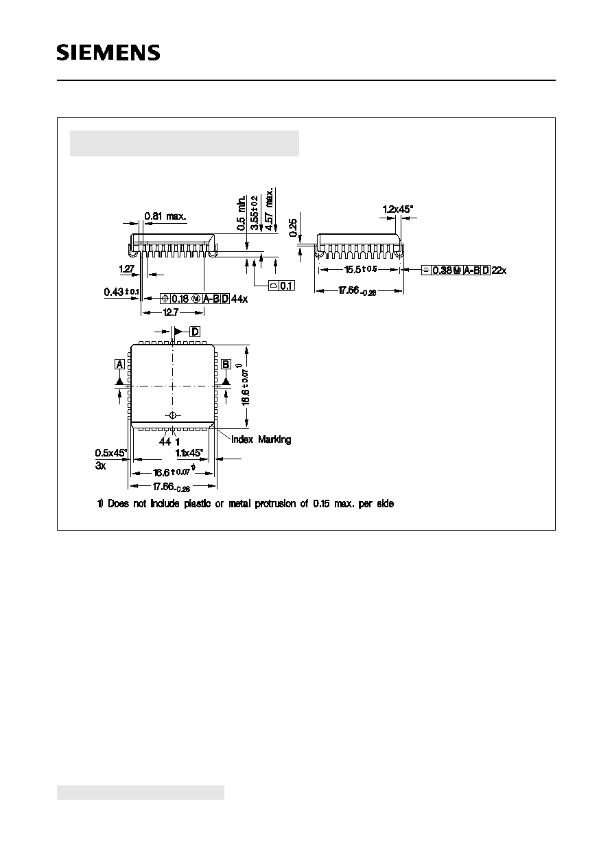
Semiconductor Group
61
C541U
Figure 38
P-LCC-44-1 Package Outline
Plastic Package, P-LCC-44-1 (SMD)
(Plastic Leaded Chip Carrier Package)
GPL05102
Sorts of Packing
Package outlines for tubes, trays etc. are contained in our
Data Book "Package Information"
Dimensions in mm
SMD = Surface Mounted Device