Semiconductor Group
1
PNP Silicon Darlington Transistors
BC 876
... BC 880
5.91
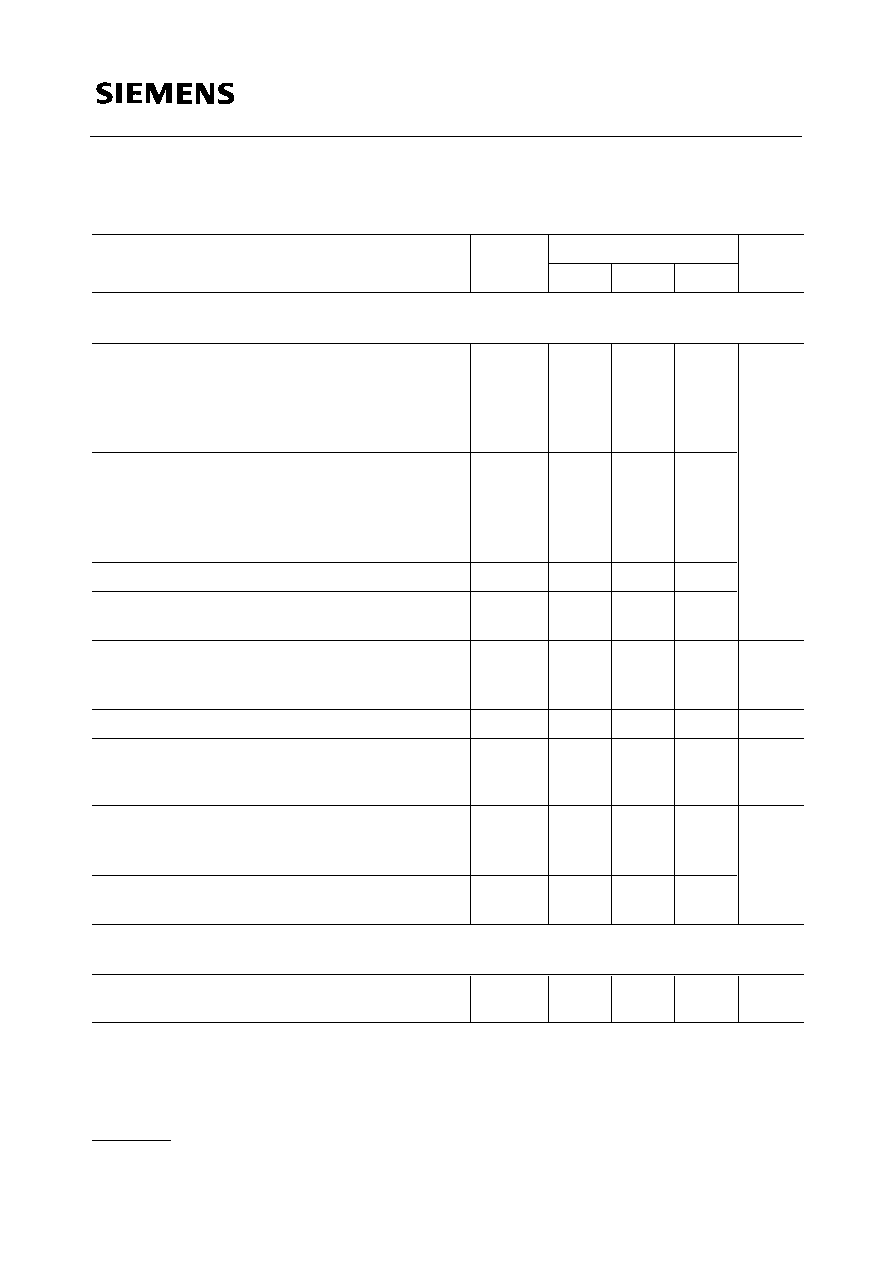
Maximum Ratings
Type
Ordering Code
Marking
Package
1)
Pin Configuration
BC 876
BC 878
BC 880
C62702-C943
C62702-C942
C62702-C941
≠
TO-92
E
C
B
1
2
3
1)
For detailed information see chapter Package Outlines.
2)
If transistors with max. 4 mm lead length are fixed on PCBs with a min. 10 mm
◊
10 mm large copper area for
the collector terminal,
R
thJA
= 125 K/W and thus
P
tot max
= 1 W at
T
A
= 25 ∞C.
3)
Mounted on Al heat sink 15 mm
◊
25 mm
◊
0.5 mm.
Parameter
Symbol
Values
Unit
Collector-emitter voltage
V
CE0
V
Peak collector current
I
CM
Collector current
I
C
A
Junction temperature
T
j
∞C
Total power dissipation,
T
C
= 90 ∞C
2)
P
tot
W
Storage temperature range
T
stg
Collector-base voltage
V
CB0
Thermal Resistance
Junction - ambient
2)
R
th JA
156
K/W
1
2
0.8 (1)
150
≠ 65 ... + 150
Emitter-base voltage
V
EB0
Base current
I
B
mA
100
45
60
60
80
BC 876
BC 878
Peak base current
I
BM
200
80
100
BC 880
5
Junction - case
3)
R
th JC
75
q
High current gain
q
High collector current
q
Low collector-emitter saturation voltage
q
Complementary types: BC 875, BC 877,
BC 879 (NPN)
Semiconductor Group
2
BC 876
... BC 880
Electrical Characteristics
at
T
A
= 25 ∞C, unless otherwise specified.
DC current gain
I
C
= 150 mA;
V
CE
= 10 V
1)
I
C
= 500 mA;
V
CE
= 10 V
1)
V
Collector-emitter breakdown voltage
I
C
= 50 mA
BC 876
BC 878
BC 880
V
(BR)CE0
45
60
80
≠
≠
≠
≠
≠
≠
nA
µ
A
Collector cutoff current
V
CB
=
V
CBmax
V
CB
=
V
CBmax
,
T
A
= 150 ∞C
I
CB0
≠
≠
≠
≠
100
20
Unit
Values
Parameter
Symbol
min.
typ.
max.
DC characteristics
Collector-base breakdown voltage
I
C
= 100
µ
A
BC 876
BC 878
BC 880
V
(BR)CB0
60
80
100
≠
≠
≠
≠
≠
≠
Emitter-base breakdown voltage,
I
E
= 100
µ
A
V
(BR)EB0
5
≠
≠
≠
h
FE
1000
2000
≠
≠
≠
≠
Base-emitter saturation voltage
1)
I
C
= 1000 mA;
I
B
= 1 mA
V
BEsat
≠
≠
2.2
nA
Emitter cutoff current,
V
EB
= 4 V
I
EB0
≠
≠
100
MHz
Transition frequency
I
C
= 200 mA,
V
CE
= 5 V,
f
= 20 MHz
f
T
≠
150
≠
AC characteristics
V
Collector-emitter saturation voltage
1)
I
C
= 500 mA,
I
B
= 0.5 mA
I
C
= 1000 mA,
I
B
= 1 mA
V
CEsat
≠
≠
≠
≠
1.3
1.8
Collector cutoff current
V
CE
= 0.5
◊
V
CEmax
I
CE0
≠
≠
500
1)
Pulse test:
t
300
µ
s,
D
2 %.