Semiconductor Group
508
SIPMOS
Æ
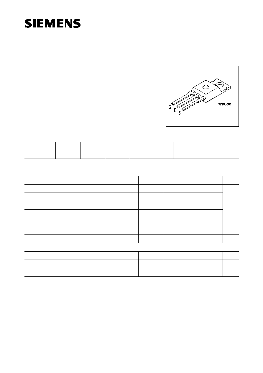
Power Transistor
BUZ 205
Maximum Ratings
Type
V
DS
I
D
R
DS (on)
Package
1)
Ordering Code
BUZ 205
400 V
6.0 A
1.0
TO-220 AB
C67078-A1401-A2
Parameter
Symbol
Values
Unit
Continuous drain current,
T
C
= 35 ∞C
I
D
6.0
A
Pulsed drain current,
T
C
= 25 ∞C
I
D puls
24
Drain-source voltage
V
DS
400
V
Drain-gate voltage,
R
GS
= 20 k
V
DGR
400
Gate-source voltage
V
GS
±
20
Power dissipation,
T
C
= 25 ∞C
P
tot
75
W
Operating and storage temperature range
T
j
,
T
stg
≠ 55 ... + 150
∞C
Thermal resistance, chip-case
R
th JC
1.67
K/W
DIN humidity category, DIN 40 040
E
≠
IEC climatic category, DIN IEC 68-1
55/150/56
q
N channel
q
Enhancement mode
q
FREDFET
1) See chapter Package Outlines.

Semiconductor Group
509
BUZ 205
Electrical Characteristics
at
T
j
= 25 ∞C, unless otherwise specified.
Parameter
Symbol
Values
Unit
min.
typ.
max.
Static characteristics
Drain-source breakdown voltage
V
GS
= 0 V,
I
D
= 0.25 mA
V
(BR) DSS
400
≠
≠
V
Gate threshold voltage
V
GS
=
V
DS
,
I
D
= 1 mA
V
GS (th)
2.1
4.0
4.0
Zero gate voltage drain current
V
DS
= 400 V,
V
GS
= 0 V
T
j
=
25 ∞C
T
j
= 125 ∞C
I
DSS
≠
≠
20
100
250
1000
µ
A
Gate-source leakage current
V
GS
= 20 V,
V
DS
= 0 V
I
GSS
≠
10
100
nA
Drain-source on-resistance
V
GS
= 10 V,
I
D
= 4.0 A
R
DS (on)
≠
0.9
1.0
Dynamic characteristics
Forward transconductance
V
DS
2 x
I
D
x
R
DS(on)max
,
I
D
= 4.0 A
g
fs
1.7
2.9
≠
S
Input capacitance
V
GS
= 0 V,
V
DS
= 25 V,
f
= 1 MHz
C
iss
≠
1500
2000
pF
Output capacitance
V
GS
= 0 V,
V
DS
= 25 V,
f
= 1 MHz
C
oss
≠
120
180
Reverse transfer capacitance
V
GS
= 0 V,
V
DS
= 25 V,
f
= 1 MHz
C
rss
≠
35
60
Turn-on time
t
on
, (
t
on
=
t
d (on)
+
t
r
)
V
DD
= ≠ 30 V,
V
GS
= 10 V,
I
D
= 2.7 A,
R
GS
= 50
t
d (on)
≠
30
45
ns
t
r
≠
40
60
Turn-off time
t
off
, (
t
off
=
t
d (off)
+
t
f
)
V
DD
= ≠ 30 V,
V
GS
= 10 V,
I
D
= 2.7 A,
R
GS
= 50
t
d (off)
≠
110
140
t
f
≠
50
65

Semiconductor Group
510
BUZ 205
Reverse diode
Continuous reverse drain current
T
C
= 25 ∞C
I
S
≠
≠
6.0
A
Pulsed reverse drain current
T
C
= 25 ∞C
I
SM
≠
≠
24
Diode forward on-voltage
I
S
= 12 A,
V
GS
= 0 V
V
SD
≠
1.3
1.6
V
Reverse recovery time
V
R
= 100 V,
I
F
=
I
DR
, d
i
F
/ d
t
= 100 A/
µ
s
t
rr
≠
180
250
ns
Reverse recovery charge
V
R
= 100 V,
I
F
=
I
DR
, d
i
F
/ d
t
= 100 A/
µ
s
Q
rr
≠
0.65
1.2
µ
C
Electrical Characteristics (cont'd)
at
T
j
= 25 ∞C, unless otherwise specified.
Parameter
Symbol
Values
Unit
min.
typ.
max.
Semiconductor Group
511
BUZ 205
Characteristics at
T
j
= 25 ∞C, unless otherwise specified.
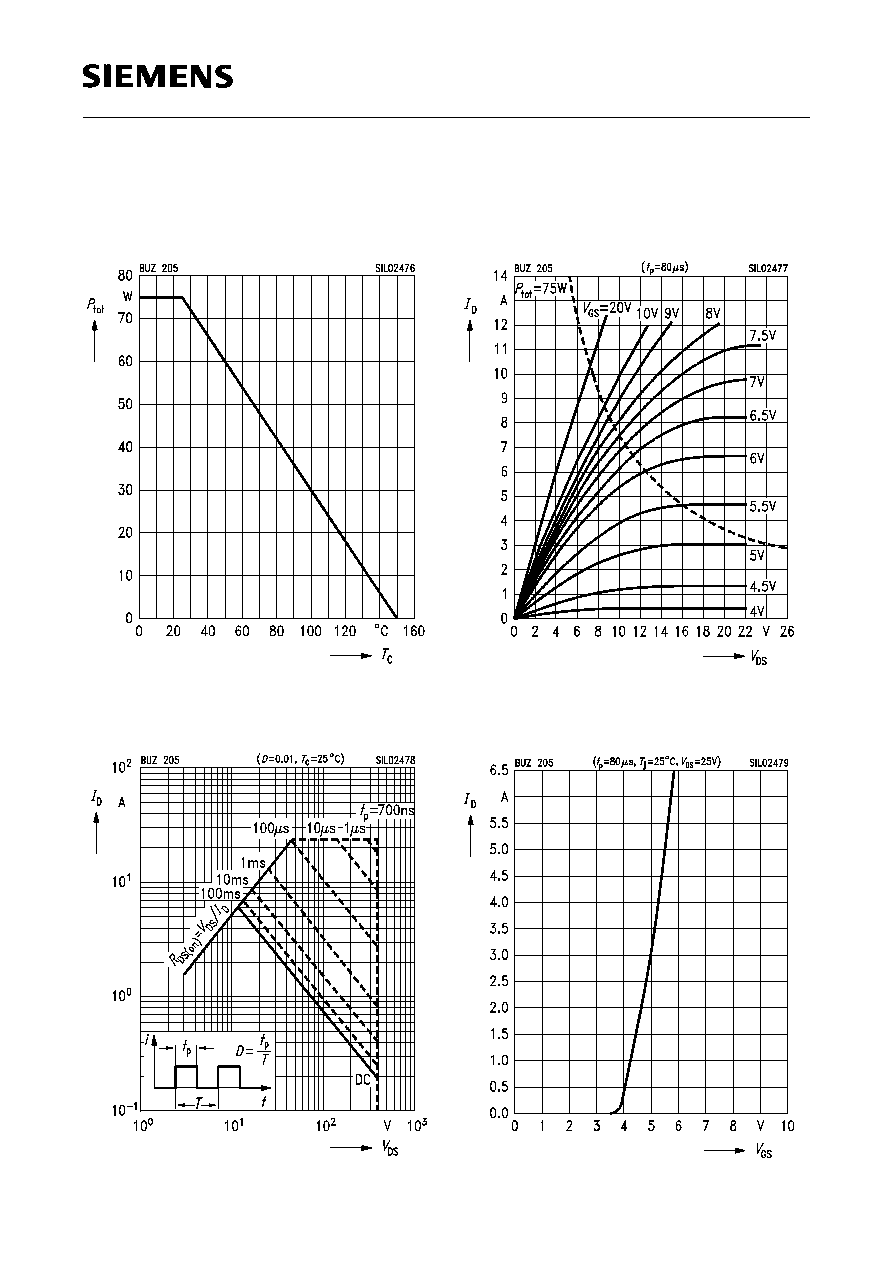
Total power dissipation
P
tot
=
f
(
T
C
)
Typ. output characteristics
I
D
=
f
(
V
DS
)
parameter:
t
p
= 80
µ
s
Safe operating area
I
D
=
f
(
V
DS
)
parameter:
D
= 0.01,
T
C
= 25 ∞C
Typ. transfer characteristics
I
D
=
f
(
V
GS
)
parameter:
t
p
= 80
µ
s,
V
DS
= 25 V
Semiconductor Group
512
BUZ 205
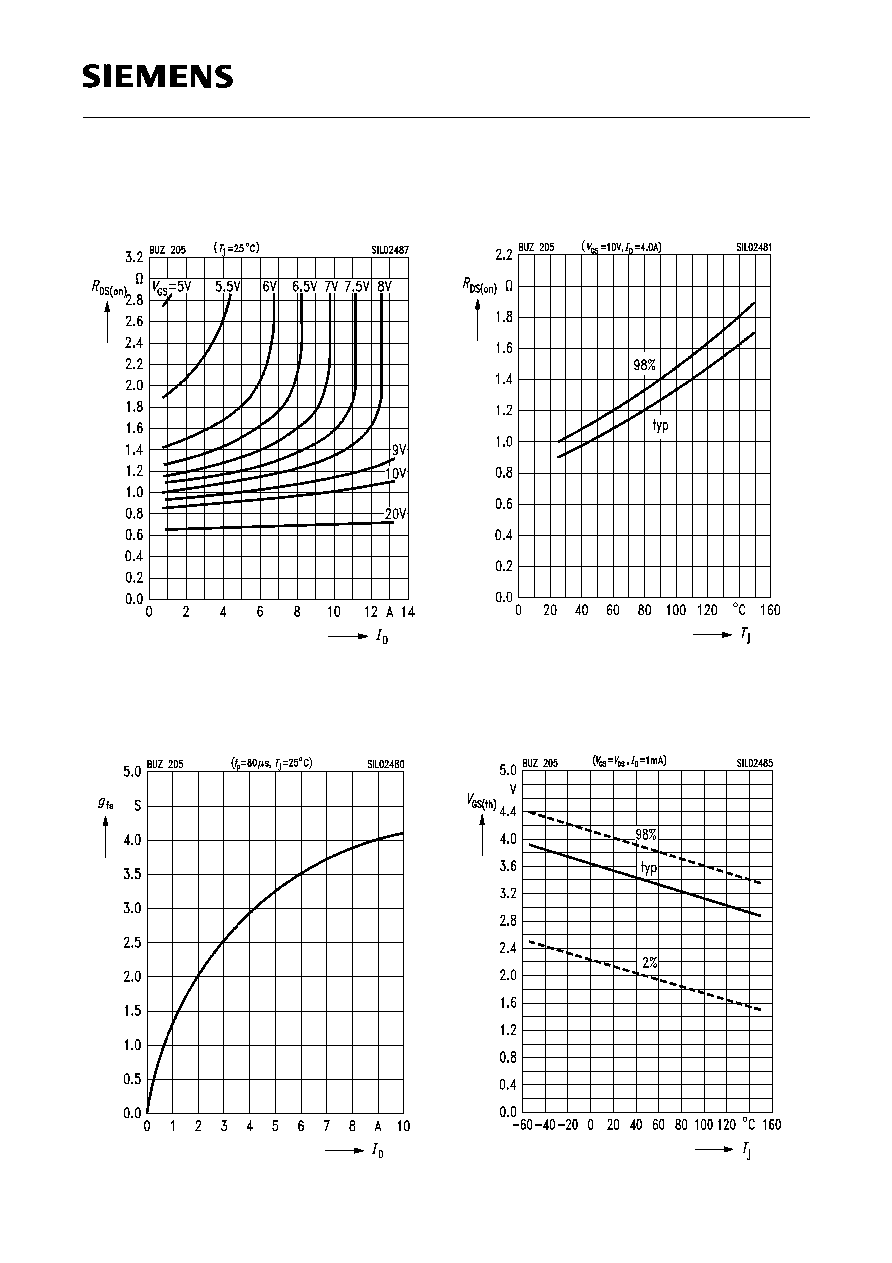
Typ. drain-source on-resistance
R
DS (on)
=
f
(
I
D
)
parameter:
V
GS
Typ. forward transconductance
g
fs
=
f
(
I
D
)
parameter:
t
p
= 80
µ
s
Drain-source on-resistance
R
DS (on)
=
f
(
T
j
)
parameter:
I
D
= 4.0 A,
V
GS
= 10 V, (spread)
Gate threshold voltage
V
GS (th)
=
f
(
T
j
)
parameter:
V
GS
=
V
DS
,
I
D
= 1 mA, (spread)