Semiconductor Group
1
07/96
BUZ 346
Not for new design
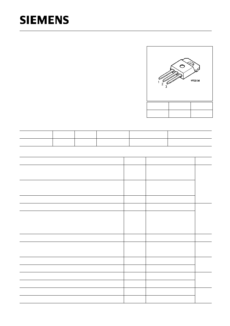
SIPMOS
Æ
Power Transistor
∑ N channel
∑ Enhancement mode
∑ Avalanche-rated
Pin 1
Pin 2
Pin 3
G
D
S
Type
V
DS
I
D
R
DS(on)
Package
Ordering Code
BUZ 346
50 V
58 A
0.018
TO-218 AA
C67078-S3120-A2
Maximum Ratings
Parameter
Symbol
Values
Unit
Continuous drain current
T
C
= 73 ∞C
I
D
58
A
Pulsed drain current
T
C
= 25 ∞C
I
Dpuls
232
Avalanche current,limited by
T
jmax
I
AR
58
Avalanche energy,periodic limited by
T
jmax
E
AR
4.5
mJ
Avalanche energy, single pulse
I
D
= 58 A,
V
DD
= 25 V,
R
GS
= 25
L = 21.4 µH, T
j
= 25 ∞C
E
AS
72
Gate source voltage
V
GS
±
20
V
Power dissipation
T
C
= 25 ∞C
P
tot
170
W
Operating temperature
T
j
-55 ... + 150
∞C
Storage temperature
T
stg
-55 ... + 150
Thermal resistance, chip case
R
thJC
0.74
K/W
Thermal resistance, chip to ambient
R
thJA
75
DIN humidity category, DIN 40 040
C
IEC climatic category, DIN IEC 68-1
55 / 150 / 56

Semiconductor Group
2
07/96
BUZ 346
Not for new design
Electrical Characteristics, at
T
j
= 25∞C, unless otherwise specified
Parameter
Symbol
Values
Unit
min.
typ.
max.
Static Characteristics
Drain- source breakdown voltage
V
GS
= 0 V,
I
D
= 0.25 mA,
T
j
= 25 ∞C
V
(BR)DSS
50
-
-
V
Gate threshold voltage
V
GS=
V
DS,
I
D
= 1 mA
V
GS(th)
2.1
3
4
Zero gate voltage drain current
V
DS
= 50 V,
V
GS
= 0 V,
T
j
= 25 ∞C
V
DS
= 50 V,
V
GS
= 0 V,
T
j
= 125 ∞C
I
DSS
-
-
10
0.1
100
1
µA
Gate-source leakage current
V
GS
= 20 V,
V
DS
= 0 V
I
GSS
-
10
100
nA
Drain-Source on-resistance
V
GS
= 10 V,
I
D
= 47 A
R
DS(on)
-
0.012
0.018
Semiconductor Group
3
07/96
BUZ 346
Not for new design
Electrical Characteristics, at
T
j
= 25∞C, unless otherwise specified
Parameter
Symbol
Values
Unit
min.
typ.
max.
Dynamic Characteristics
Transconductance
V
DS
2
*
I
D *
R
DS(on)max,
I
D
= 47 A
g
fs
30
42
-
S
Input capacitance
V
GS
= 0 V,
V
DS
= 25 V,
f = 1 MHz
C
iss
-
2900
4300
pF
Output capacitance
V
GS
= 0 V,
V
DS
= 25 V,
f = 1 MHz
C
oss
-
1400
2100
Reverse transfer capacitance
V
GS
= 0 V,
V
DS
= 25 V,
f = 1 MHz
C
rss
-
500
750
Turn-on delay time
V
DD
= 30 V,
V
GS
= 10 V,
I
D
= 3 A
R
GS
= 50
t
d(on)
-
55
80
ns
Rise time
V
DD
= 30 V,
V
GS
= 10 V,
I
D
= 3 A
R
GS
= 50
t
r
-
140
210
Turn-off delay time
V
DD
= 30 V,
V
GS
= 10 V,
I
D
= 3 A
R
GS
= 50
t
d(off)
-
420
560
Fall time
V
DD
= 30 V,
V
GS
= 10 V,
I
D
= 3 A
R
GS
= 50
t
f
-
250
330

Semiconductor Group
4
07/96
BUZ 346
Not for new design
Electrical Characteristics, at
T
j
= 25∞C, unless otherwise specified
Parameter
Symbol
Values
Unit
min.
typ.
max.
Reverse Diode
Inverse diode continuous forward current
T
C
= 25 ∞C
I
S
-
-
58
A
Inverse diode direct current,pulsed
T
C
= 25 ∞C
I
SM
-
-
232
Inverse diode forward voltage
V
GS
= 0 V,
I
F
= 116 A
V
SD
-
1.6
2
V
Reverse recovery time
V
R
= 30 V,
I
F=
l
S,
d
i
F
/d
t = 100 A/µs
t
rr
-
100
-
ns
Reverse recovery charge
V
R
= 30 V,
I
F=
l
S,
d
i
F
/d
t = 100 A/µs
Q
rr
-
0.3
-
µC
5
07/96
Semiconductor Group
BUZ 346
Not for new design
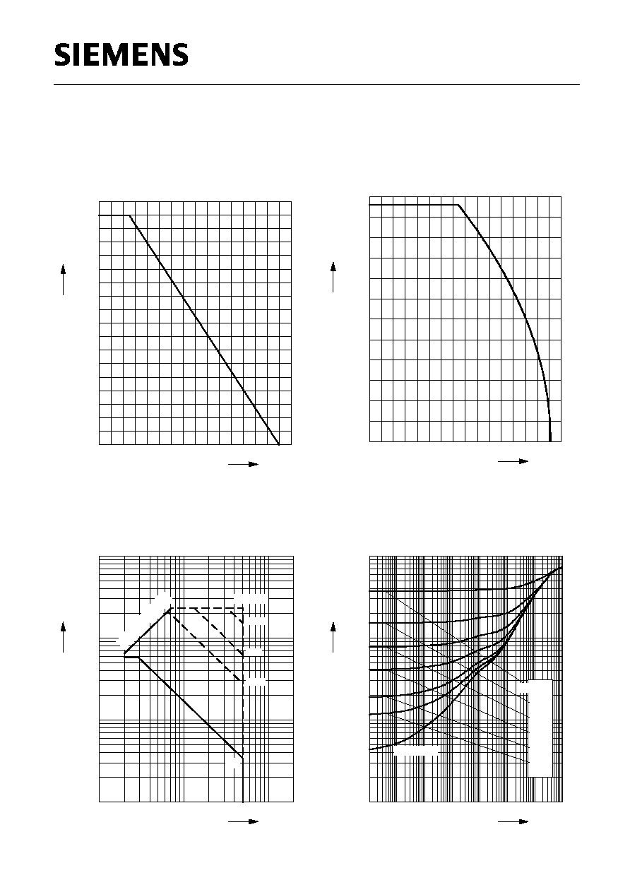
Drain current
I
D
=
(
T
C
)
parameter:
V
GS
10 V
0
20
40
60
80
100
120
∞C
160
T
C
0
5
10
15
20
25
30
35
40
45
50
A
60
I
D
Power dissipation
P
tot
=
(
T
C
)
0
20
40
60
80
100
120
∞C
160
T
C
0
20
40
60
80
100
120
140
W
180
P
tot
Safe operating area
I
D
=
(
V
DS
)
parameter:
D = 0.01, T
C
= 25∞C
0
10
1
10
2
10
3
10
A
I
D
10
0
10
1
10
2
V
V
DS
R
DS(on)
=
V
DS
/
I
D
DC
10 ms
1 ms
100 µs
t
p = 28.0µs
Transient thermal impedance
Z
th JC
=
(
t
p
)
parameter:
D = t
p
/
T
-3
10
-2
10
-1
10
0
10
K/W
Z
thJC
10
-7
10
-6
10
-5
10
-4
10
-3
10
-2
10
-1
10
0
s
t
p
single pulse
0.01
0.02
0.05
0.10
0.20
D = 0.50
Semiconductor Group
6
07/96
BUZ 346
Not for new design
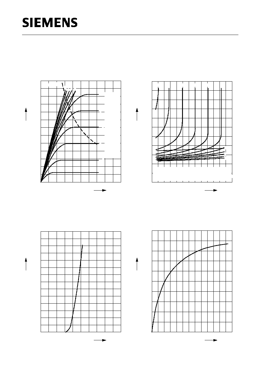
Typ. output characteristics
I
D
=
(
V
DS
)
parameter:
t
p
= 80 µs
0.0
0.5
1.0
1.5
2.0
2.5
3.0
3.5
4.0
V
5.0
V
DS
0
10
20
30
40
50
60
70
80
90
100
110
A
130
I
D
V
GS
[V]
a
a
4.0
b
b
4.5
c
c
5.0
d
d
5.5
e
e
6.0
f
f
6.5
g
g
7.0
h
h
7.5
i
i
8.0
j
j
9.0
k
k
10.0
l
P
tot
= 170W
l
20.0
Typ. drain-source on-resistance
R
DS (on)
=
(
I
D
)
parameter:
V
GS
0
20
40
60
80
100
A
130
I
D
0.000
0.005
0.010
0.015
0.020
0.025
0.030
0.035
0.040
0.045
0.055
R
DS (on)
V
GS
[V] =
a
a
4.0
b
b
4.5
c
c
5.0
d
d
5.5
e
e
6.0
f
f
6.5
g
g
7.0
h
h
7.5
i
i
8.0
j
j
9.0
k
k
10.0
l
l
20.0
Typ. transfer characteristics
I
D
=
f (V
GS
)
parameter:
t
p
= 80 µs
V
DS
2 x
I
D
x
R
DS(on)max
0
1
2
3
4
5
6
7
8
V
10
V
GS
0
5
10
15
20
25
30
35
40
45
50
55
60
A
70
I
D
Typ. forward transconductance
g
fs
=
f
(
I
D
)
parameter:
t
p
= 80 µs,
V
DS
2 x
I
D
x R
DS(on)max
0
10
20
30
40
50
A
65
I
D
0
5
10
15
20
25
30
35
40
S
50
g
fs

7
07/96
Semiconductor Group
BUZ 346
Not for new design
Gate threshold voltage
V
GS (th)
=
(
T
j
)
parameter:
V
GS
=
V
DS
,
I
D
= 1 mA
0.0
0.4
0.8
1.2
1.6
2.0
2.4
2.8
3.2
3.6
4.0
V
4.6
V
GS(th)
-60
-20
20
60
100
∞C
160
T
j
2%
typ
98%
Drain-source on-resistance
R
DS (on)
=
(
T
j
)
parameter:
I
D
= 47 A,
V
GS
= 10 V
-60
-20
20
60
100
∞C
160
T
j
0.000
0.005
0.010
0.015
0.020
0.025
0.030
0.035
0.045
R
DS (on)
typ
98%
Typ. capacitances
C = f (V
DS
)
parameter:
V
GS
= 0V,
f = 1MHz
0
5
10
15
20
25
30
V
40
V
DS
-2
10
-1
10
0
10
1
10
nF
C
C
rss
C
iss
C
oss
Forward characteristics of reverse diode
I
F
=
(
V
SD
)
parameter:
T
j
, t
p
= 80 µs
0
10
1
10
2
10
3
10
A
I
F
0.0
0.4
0.8
1.2
1.6
2.0
2.4
V
3.0
V
SD
T
j
= 25 ∞C typ
T
j
= 25 ∞C (98%)
T
j
= 150 ∞C typ
T
j
= 150 ∞C (98%)

Semiconductor Group
8
07/96
BUZ 346
Not for new design
Avalanche energy
E
AS
=
(
T
j
)
parameter:
I
D
= 58 A,
V
DD
= 25 V
R
GS
= 25
,
L = 21.4 µH
20
40
60
80
100
120
∞C
160
T
j
0
5
10
15
20
25
30
35
40
45
50
55
60
65
mJ
75
E
AS
Typ. gate charge
V
GS
=
(
Q
Gate
)
parameter:
I
D puls
= 87 A
0
20
40
60
80
100
120
nC
160
Q
Gate
0
2
4
6
8
10
12
V
16
V
GS
DS max
V
0,8
DS max
V
0,2
Drain-source breakdown voltage
V
(BR)DSS
=
(
T
j
)
-60
-20
20
60
100
∞C
160
T
j
45
46
47
48
49
50
51
52
53
54
55
56
57
58
V
60
V
(BR)DSS
Semiconductor Group
9
07/96
BUZ 346
Not for new design
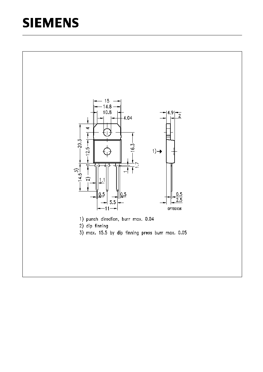
Package Outlines
TO-218 AA
Dimension in mm