
GaAs MMIC
CGY 180
_________________________________________________________________________________________________________
Siemens Aktiengesellschaft
pg. 1/15
21.02.96
HL EH PD 21
Datasheet
* Power amplifier for DECT and PCS application
* Fully integrated 3 stage amplifier
* Operating voltage range: 2.7 to 6 V
* Overall power added efficiency 35 %
* Input matched to 50
, simple output match
ESD:
Electrostatic discharge sensitive device,
observe handling precautions!
Type
Marking
Ordering code
(taped)
Package 1)
CGY 180
CGY 180
Q68000-A8882
MW 12
Maximum ratings
Characteristics
Symbol
max. Value
Unit
Positive supply voltage
VD
8
V
Negative supply voltage
2
)
VG
-8
V
Supply current
ID
1.2
A
Maximum input power
Pin,max
10
dBm
Channel temperature
TCh
150
�C
Storage temperature
Tstg
-55...+150
�C
Total power dissipation
(Ts < 81 �C)
Ts: Temperature at soldering point
Ptot
2.3
W
Pulse peak power
PPulse
9.5
W
Thermal Resistance
Channel-soldering point
RthChS
30
K/W
1) Plastic body identical to SOT 223,
dimensions see chapter Package Outlines
2) V
G
= -8V only in combination with V
TR
= 0V; V
G
= -6V while V
TR
0V

GaAs MMIC
CGY 180
_________________________________________________________________________________________________________
Siemens Aktiengesellschaft
pg. 2/15
21.02.96
HL EH PD 21
Functional Block Diagram:
Pin #
Configuration
1
VTR
Control voltage for transmit (0V) / receive (open) mode
2
VG
Negative voltage at control circuit (-4V...-8V)
3
GND2
RF and DC ground of the 2nd and 3rd stage
4
GND2
RF and DC ground of the 2nd and 3rd stage
5
GND2
RF and DC ground of the 2nd and 3rd stage
6
GND1
RF and DC ground of the 1st stage
7
RFin
RF input power
8
VD1
Pos. drain voltage of the 1st stage
9
VD2
Pos. drain voltage of the 2nd stage
10
GND2
RF and DC ground of the 2nd and 3rd stage
11
VD3, Pout Pos. drain voltage of the 3rd stage, RF output power
12
n.c.
Control
circuit
VTR
Pin
Pout
GND1
GND2
VD1
VD2
VD3
VG
(2)
(8)
(9)
(1)
(6)
(11)
(3,4,5,10)
(11)
(7)

GaAs MMIC
CGY 180
_________________________________________________________________________________________________________
Siemens Aktiengesellschaft
pg. 3/15
21.02.96
HL EH PD 21
Control circuit:
VG supply: Negative voltage (stabilization is not necessary) in the range of -4V...-8V.
VTR supply: During transmit operation: 0V., negative supply current 1mA...2.5mA.
During receive operation: not connected (shut off mode)
The operation current ID of CGY 180 is adjusted by the internal control circuit.
DC characteristics
Characteristics
Symbol Conditions
min
typ
max
Unit
Drain current stage 1
IDSS1
VD=3V, VG=0V, VTR n.c.
150
220
320
mA
stage 2
IDSS2
150
220
320
mA
stage 3
IDSS3
675
1000
1440
mA
Drain current with
active current control
ID
VD=3V, VG=-4V, VTR=0V
290
450
650
mA
Transconductance
gfs1
VD=3V, ID=90mA
80
100
140
mS
(stage 1 - 3)
gfs2
VD=3V, ID=90mA
80
100
140
mS
gfs3
VD=3V, ID=400mA
360
500
630
mS
Pinch off voltage
Vp
VD=3V, ID<170
�
A
(all stages)
-3.8
-2.8
-1.8
V

GaAs MMIC
CGY 180
_________________________________________________________________________________________________________
Siemens Aktiengesellschaft
pg. 4/15
21.02.96
HL EH PD 21
Electrical characteristics
(TA = 25�C , f=1.89 GHz, ZS=ZL=50 Ohm, VD=3.0V, VG=-4V, VTR pin connected to
ground, unless otherwise specified)
Characteristics
Symbol
min
typ
max
Unit
Supply current
Pin = 0 dBm
IDD
-
450
-
mA
Negative supply current
(transmit operation)
IG
-
1
2.5
mA
Shut-off current
VTR n.c.
ID
-
50
180
�A
Negative supply current
(shut off mode, VTR pin n.c.)
IG
-
10
50
�A
Gain
Pin = -20dBm
G
28
30
-
dB
Output Power
Pin = 0 dBm
Po
25.5
27
-
dBm
Output Power
VD=5V; Pin = 0 dBm
Po
-
30
-
dBm
Overall Power added Efficiency
Pin = 0 dBm
30
35
-
%
Harmonics
(Pin =0dBm)
2f
0
VD=3V; (Pout =27dBm)
3f
0
-
-
-
-
-
-
-28
-25
dBc
Harmonics
(Pin =0dBm)
2f
0
VD=5V; (Pout =30dBm)
3f
0
-
-
-
-
-
-
-25
-22
dBc
Input VSWR V
D=3V;
-
-
2 : 1
2.5 : 1
-
Third order intercept point
VD=3V; pulsed with a duty cycle of 10%;
f
1
=1.8900GHz; f
2
=1.891728GHz;
IP
3
-
33.5
-
dBm
Third order intercept point
VD=4.8V; pulsed with a duty cycle of 10%;
f
1
=1.8900GHz; f
2
=1.891728GHz;
IP
3
-
38.5
-
dBm
Load mismatch
Pin=0dBm, VD
6V, Z
S
=50 Ohm,
Load VSWR = 20:1 for all phase,
VTR=0V, VG=-4V
-
No module damage
for 10 sec.
-
Stability
Pin=0dBm, VD=2-7V, Z
S
=50 Ohm,
Load VSWR = 3:1 for all phase,
VTR=0V, VG=-4V
-
All spurious output
more than 60 dB below
desired signal level
-

GaAs MMIC
CGY 180
_________________________________________________________________________________________________________
Siemens Aktiengesellschaft
pg. 5/15
21.02.96
HL EH PD 21
DC - characteristics
Input characteristics - typical measured values of stage 1 and 2 , VD1 or VD2=3V
Output characteristics - typical measured values of stage 1 and 2
0
0,02
0,04
0,06
0,08
0,1
0,12
0,14
0,16
0,18
0,2
0,22
0,24
0,26
-4
-3,8
-3,6
-3,4
-3,2
-3
-2,8
-2,6
-2,4
-2,2
-2
-1,8
-1,6
-1,4
-1,2
-1
-0,8
-0,6
-0,4
-0,2
0
VG[V]
ID[A]
low current
medium current
high current
0
0,02
0,04
0,06
0,08
0,1
0,12
0,14
0,16
0,18
0,2
0,22
0
0,2 0,4 0,6 0,8
1
1,2 1,4 1,6 1,8
2
2,2 2,4 2,6 2,8
3
3,2 3,4 3,6 3,8
4
4,2 4,4 4,6 4,8
5
5,2 5,4 5,6 5,8
6
VD[V]
ID[A]
0V
-0.2V
-0.3V
-0.5V
-0.7V
-0.8V
-1.0V
-1.2V
-1.3V
-1.5V
-1.7V
-1.9V
-2.1V
-2.3V
-2.5V

GaAs MMIC
CGY 180
_________________________________________________________________________________________________________
Siemens Aktiengesellschaft
pg. 6/15
21.02.96
HL EH PD 21
Input characteristics - typical measured values of stage 3, VD3 = 3V
Output characteristics - typical measured values of stage 3
0
0,1
0,2
0,3
0,4
0,5
0,6
0,7
0,8
0,9
1
1,1
1,2
1,3
-4
-3,8
-3,6
-3,4
-3,2
-3
-2,8
-2,6
-2,4
-2,2
-2
-1,8
-1,6
-1,4
-1,2
-1
-0,8
-0,6
-0,4
-0,2
0
VG[V]
ID[A]
low current
medium current
high current
0
0,1
0,2
0,3
0,4
0,5
0,6
0,7
0,8
0,9
1
1,1
0
0,2 0,4 0,6 0,8
1
1,2 1,4 1,6 1,8
2
2,2 2,4 2,6 2,8
3
3,2 3,4 3,6 3,8
4
4,2 4,4 4,6 4,8
5
5,2 5,4 5,6 5,8
6
VD[V]
ID[A]
0V
-0.1V
-0.2V
-0.3V
-0.4V
-0.6V
-0.7V
-0.9V
-1.1V
-1.3V
-1.5V
-1.7V
-1.9V
-2.1V
-2.3V
-2.5V

GaAs MMIC
CGY 180
_________________________________________________________________________________________________________
Siemens Aktiengesellschaft
pg. 7/15
21.02.96
HL EH PD 21
Output power and power added efficiency
pulsed mode: ton=1ms, duty cycle 10%
P
out
and PAE vs. Pin
f = 1.89 GHz , VD = 5 V, VG=-4V, VTR=0V
0
5
10
15
20
25
30
35
40
45
-20
-15
-10
-5
0
5
10
P
in
[dBm]
P
out
[dBm]
PAE [%]
Pout [dBm]
PAE [%]
P
out
and PAE vs. Pin
f = 1.89 GHz , VD = 3 V, VG=-4V, VTR=0V
12
13
14
15
16
17
18
19
20
21
22
23
24
25
26
27
28
29
30
-20
-18
-16
-14
-12
-10
-8
-6
-4
-2
0
2
4
6
P
in
[dBm]
Pout[dBm]
0
2
4
6
8
10
12
14
16
18
20
22
24
26
28
30
32
34
36
PAE [%]
Pout [dBm]
PAE [%]

GaAs MMIC
CGY 180
_________________________________________________________________________________________________________
Siemens Aktiengesellschaft
pg. 8/15
21.02.96
HL EH PD 21
Gain vs. frequency
VG=-4V, VTR=0V
3V Pin=0dBm
3V Pin=-20dBm
5V Pin=-20dBm
5V Pin=0dBm
GAIN vs. DRAIN VOLTAGE
f=1.89 GHz, VD=3V, VG=-4V, VTR=0V
25
26
27
28
29
30
31
32
33
2
3
4
5
6
V
D
[V]
Gain [dB]
Gain [dB] Pin= 0dBm
Gain [dB] Pin =-20dBm

GaAs MMIC
CGY 180
_________________________________________________________________________________________________________
Siemens Aktiengesellschaft
pg. 9/15
21.02.96
HL EH PD 21
Output power control vs. VTR
0
5
10
15
20
25
30
35
0
0,5
1
1,5
2
-VTR [V]
Pout [dBm]
0
100
200
300
400
500
600
700
Id [mA]
Pout (Vd=4.5V) [dBm]
Pout (Vd=3V) [dBm]
ID (Vd=4.5V) [mA]
ID (Vd=3V) [mA]
Total Power Dissipation Ptot=f(T
S
)

GaAs MMIC
CGY 180
_________________________________________________________________________________________________________
Siemens Aktiengesellschaft
pg. 10/15
21.02.96
HL EH PD 21
Permissible pulse load P
tot_max
/P
tot_DC
= f(t_p)

GaAs MMIC
CGY 180
_________________________________________________________________________________________________________
Siemens Aktiengesellschaft
pg. 11/15
21.02.96
HL EH PD 21
Test circuit board:
The following impedances of the bias circuit
should be seen from the CGY180 ports:
(values measured at f=1.89 GHz)
Size: 20 x 25 mm; In, Out: 50 Ohm
Principal circuit:
8
9
11
CGY 180
8
= 0.97 / 96�
9
= 0.96 / 142�
11
= 0.94 / -134�
8
9
11
Control
circuit
VTR
Pin
Pout
GND1
GND2
VD1
VD2
VD3
VG
(2)
(8)
(9)
(1)
(6)
(11)
(3,4,5,10)
(11)
(7)
1nF
1nF
1nF
68pF
6.8pF
1.5pF
4.7uF
1nF
Vg
+Vd
Out
In
VTR
CGY180

GaAs MMIC
CGY 180
_________________________________________________________________________________________________________
Siemens Aktiengesellschaft
pg. 12/15
21.02.96
HL EH PD 21
Output power at different temperatures*
Power added efficiency at different temperatures*
*)measured with a CGY180 test circuit board (see page 11) VD=3V, VG=-4V, VTR=0V
16
18
20
22
24
26
28
30
-12
-10
-8
-6
-4
-2
0
2
4
Pin [dBm]
Pout [dBm]
Pout(-20�C) [dBm]
Pout(+20�C) [dBm]
Pout(+70�C) [dBm]
0
5
10
15
20
25
30
35
40
-12
-10
-8
-6
-4
-2
0
2
4
Pin [dBm]
PAE [%]
PAE(-20�C) [%]
PAE(+20�C) [%]
PAE(+70�C) [%]
GaAs MMIC
CGY 180
_________________________________________________________________________________________________________
Siemens Aktiengesellschaft
pg. 13/15
21.02.96
HL EH PD 21
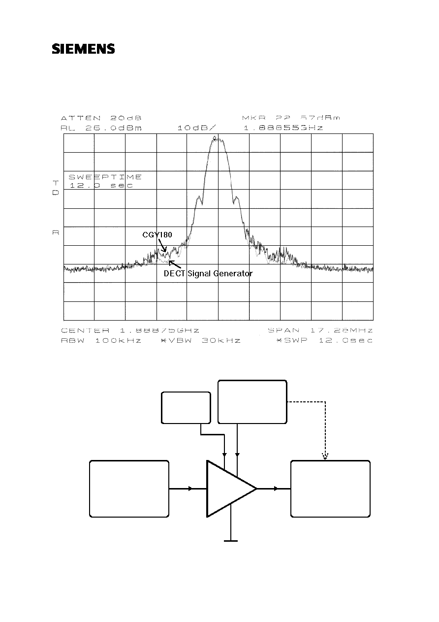
Emissions due to modulation:*
Spectrum of amplified DECT signal
Measurement was done with the following equipment:
DECT Signal
Generator
Spectrum
Analyzer
HP 8561E
Trigger
gate delay 3�s
gate length 1ms
VG
VD
VTR
IN
OUT
-4V
Pulsed Power
Supply
VD=3V
pulsed with a duty cycle of 10%
ton=1ms
CGY180
negative supply
voltage
Pin=0dBm
ROHDE&SCHWARZ SME03
*)measured with a CGY180 test circuit board (see page 11) VD=3V, VG=-4V, VTR=0V

GaAs MMIC
CGY 180
_________________________________________________________________________________________________________
Siemens Aktiengesellschaft
pg. 14/15
21.02.96
HL EH PD 21
APPLICATION - HINTS
1. CW - capability of the CGY180
1.1 VD = 3 V
Proving the possibility of CW - operations there must be known the total power dissipation of the
device. This value can be found as a function of the temperature in the datasheet (page 8/14). The
CGY180 has a maximum total power dissipation of Ptot = 2.3 W.
As an example we take the operating point with a drain voltage VD = 3 V. The possible ratings of
the drain current adjusted by the internal current control of the CGY180
( V
G
= -4 V, V
TR
= 0 V ) are shown in the following table.
Min.
Typ.
Max.
ID / mA
325
450
650
At worst case you see a current of ID = 650 mA. So the maximum DC - power can be calculated to
P
V
I
W
DC
D
D
=
=
1 95
.
This value is smaller than 2.3W and CW - operation is possible.
1.2 VD = 4 V
If you want to use the whole capability of the CGY180, you must consider the power added
efficiency PAE. You want to take an operation point of V
D
= 4 V. Now there will be a higher
current than at V
D
= 3 V. We assume a current of ID = 650 mA and a PAE = 35 %. With these
values the DC - power is P
DC
= 2.6 W. That exeeds the PtotDC of 2.3 W. Decoupling RF-Power
from the CGY180 results in less power dissipation of the device. This is directly correlated with the
achieved PAE. To calculate total power dissipation use the formula
:
(
)
P
P
PAE
totDC
DC
=
-
1
.
P
tot
for the used operating point shown above will be
P
W
W
tot
=
-
=
2 6
1 0 35
1 69
.
(
.
)
.
.
It is possible to use the CGY180 for CW - operations up to a drain voltage of V
D
= 4 V, if at the
same time a PAE of 35% is achieved.
The calculation can be done for any operating point to prove the capability of CW - operation.

GaAs MMIC
CGY 180
_________________________________________________________________________________________________________
Siemens Aktiengesellschaft
pg. 15/15
21.02.96
HL EH PD 21
2. Not using the internal current control
If you don' t want to use the internal current control, it is recommended to connect the negative
supply voltage at pin 1 ( VTR ) instead of pin 2 ( VG ).
3. Biasing and use considerations
In all cases, RF input power should not be applied until the bias voltages have been applied, and RF
input power should be turned off prior to removing the bias voltages. Bias application should be
timed such that gate voltage ( VGG ) is always applied before the drain voltages
( VDD ), and when returning to the standby mode, gate voltage should only be removed once the
drain voltages have been removed.