 | –≠–ª–µ–∫—Ç—Ä–æ–Ω–Ω—ã–π –∫–æ–º–ø–æ–Ω–µ–Ω—Ç: FEF4065 | –°–∫–∞—á–∞—Ç—å:  PDF PDF  ZIP ZIP |

ICs for Communications
High Voltage Subscriber Line IC
HV-SLIC
PEB/F 4065 Version 3.0
Data Sheet 03.98
DS 1
htt
p:/
/ww
w
.sie
m
en
s.d
e/
Se
m
ic
on
du
ct
or
/

SLICOFI
Æ
is a registered trademark of SIEMENS AG.
For questions on technology, delivery and prices please contact the Semiconductor Group Offices
in Germany or the Siemens Companies and Representatives worldwide: see our webpage at http:/
/www.siemens.de/Semiconductor/address/address.htm.
PEB/F 4065
Revision History:
Current Version: 03.98
Previous Version:
01.96
Page
(in previous
Version)
Page
(in current
Version)
Subjects (major changes since last revision)
Edition 03.98
Published by Siemens AG,
HL SP,
Balanstraþe 73,
81541 M¸nchen
©
Siemens AG 1998.
All Rights Reserved.
Attention please!
As far as patents or other rights of third parties are concerned, liability is only assumed for components, not for
applications, processes and circuits implemented within components or assemblies.
The information describes the type of component and shall not be considered as assured characteristics.
Terms of delivery and rights to change design reserved.
Due to technical requirements components may contain dangerous substances. For information on the types in
question please contact your nearest Siemens Office, Semiconductor Group.
Siemens AG is an approved CECC manufacturer.
Packing
Please use the recycling operators known to you. We can also help you ≠ get in touch with your nearest sales
office. By agreement we will take packing material back, if it is sorted. You must bear the costs of transport.
For packing material that is returned to us unsorted or which we are not obliged to accept, we shall have to invoice
you for any costs incurred.
Components used in life-support devices or systems must be expressly authorized for such purpose!
Critical components
1
of the Semiconductor Group of Siemens AG, may only be used in life-support devices or
systems
2
with the express written approval of the Semiconductor Group of Siemens AG.
1 A critical component is a component used in a life-support device or system whose failure can reasonably be
expected to cause the failure of that life-support device or system, or to affect its safety or effectiveness of that
device or system.
2 Life support devices or systems are intended (a) to be implanted in the human body, or (b) to support and/or
maintain and sustain human life. If they fail, it is reasonable to assume that the health of the user may be en-
dangered.

PEB/F 4065
Table of Contents
Page
Semiconductor Group
3
1998-03-01
1
Overview . . . . . . . . . . . . . . . . . . . . . . . . . . . . . . . . . . . . . . . . . . . . . . . . . . .4
1.1
Features . . . . . . . . . . . . . . . . . . . . . . . . . . . . . . . . . . . . . . . . . . . . . . . . . . .4
1.2
Functional Description . . . . . . . . . . . . . . . . . . . . . . . . . . . . . . . . . . . . . . . . .5
1.3
Pin Description . . . . . . . . . . . . . . . . . . . . . . . . . . . . . . . . . . . . . . . . . . . . . .9
2
Electrical Characteristics. . . . . . . . . . . . . . . . . . . . . . . . . . . . . . . . . . . . .11
2.1
Absolute Maximum Ratings . . . . . . . . . . . . . . . . . . . . . . . . . . . . . . . . . . . .11
2.2
Operating Range . . . . . . . . . . . . . . . . . . . . . . . . . . . . . . . . . . . . . . . . . . . .12
2.3
Thermal Resistances . . . . . . . . . . . . . . . . . . . . . . . . . . . . . . . . . . . . . . . . .12
2.4
Electrical Parameters . . . . . . . . . . . . . . . . . . . . . . . . . . . . . . . . . . . . . . . .13
2.5
AC-Characteristics . . . . . . . . . . . . . . . . . . . . . . . . . . . . . . . . . . . . . . . . . . .18
3
Package Outlines . . . . . . . . . . . . . . . . . . . . . . . . . . . . . . . . . . . . . . . . . . .29

P-DSO-20-5
Semiconductor Group
4
1998-03-01
High Voltage Subscriber Line IC
HV-SLIC
PEB/F 4065
Version 1.1
SPT
Type
Ordering Code
Package
PEB/F 4065
on request
P-DSO-20-5
1
Overview
The High Voltage Subscriber Line IC PEB 4065 is a
rugged and reliable interface between the telephone
line and the SLICOFI, a low voltage Subscriber Line
Interface and Codec Filter IC. It is fabricated in a Smart
Power Technology offering a breakthrough voltage of
at least 170 V.
The PEB 4065 provides battery feeding between
≠ 24 V and ≠ 80 V and internal ringing injection with a
differential ring voltage up to 85 Vrms. In order to
achieve these high amplitudes an auxiliary positive battery voltage is used during
ringing. This voltage can also be applied in order to drive very long telephone lines.
The SLIC is designed for a voltage feeding ≠ current sensing line interface concept and
provides sensing of transversal and longitudinal current on both wires.
A power-down mode offers reduced power consumption at full functionality; in the power
denial mode the device is switched off turning the line outputs to a high impedance state.
1.1
Features
∑ High voltage line feeding
∑ Internal ring and metering signal injection
∑ Sensing of transversal and longitudinal line current
∑ Reliable 170 V Smart Power Technology
∑ Battery voltage ≠ 24 V ... ≠ 80 V
∑ Boosted battery mode for long telephone lines
and up to 85 Vrms balanced ringing
∑ Polarity reversal
∑ Small P-DSO-20-5 power package

PEB/F 4065
Overview
Semiconductor Group
5
1998-03-01
1.2
Functional Description
Figure 1
Block Diagram
The PEB 4065 supports AC and DC control loops based on feeding a voltage
V
ab
to the
line and sensing the transversal line current
I
ab
(Figure 2).
It converts a unipolar input voltage
V
2W
into a differential output voltage
V
ab
with an AC
receiving gain of
Gr
=
V
abAC
/
V
2WAC
= 40.
This is accomplished by converting the input voltage to a current which is used to
transpose the low voltage signals of the interface to the high voltage line feeding section.
This current is reconverted to two voltages of opposite phase which are referenced to
the positive and negative supply voltage, respectively. Thus the differential DC
line-voltage in all normal polarity modes except ringing is related to the input voltage by
V
abDC
=
V
BAT
≠
V
HINT
+
V
fix
≠ 40
◊
V
2WDC
V
BAT
negative battery voltage
V
HINT
internal positive supply voltage
V
fix
internal voltage drop of supply filter (appr. 2 V).
Depending on the operation mode,
V
HINT
is switched either to
V
H
(
V
HINT
=
V
H
≠ 1 V) or to
BGND (
V
HINT
= ≠ 0.5 V) via the supply switch.
ITB10371
Buffer
Buffer
Current sensor
Differential
Supply
Control
V/I Converter
Reference
Switch
I/V-Converter
Supply
C1
C2
V
PDN
2W
AGND
BAT
V
V
BIM
SS
V
DD
V
RING
TIP
V
ab
BGND
HINT
V
a
b
V
BAT
V
H
T
L

PEB/F 4065
Overview
Semiconductor Group
6
1998-03-01
Controlled by C2, the polarity of
V
ab
can be reversed and the DC-line-voltage then is
V
abDC
= ≠ (
V
BAT
≠
V
HINT
+
V
fix
≠ 40
◊
V
2WDC
).
The transversal and longitudinal currents are measured in the buffers and scaled images
are provided at the
I
T
and
I
L
pin, respectively:
I
T
= (
I
a
+
I
b
)/100 =
I
ab
/50
I
L
= ≠ (
I
a
≠
I
b
)/100 = ≠
I
Long
/50.
The PEB 4065 operates in four modes controlled by ternary logic signals at the C1 and
C2 input. Additionally, in the active modes a polarity reversal of the output voltage can
be programmed (see Table 1).
Power down (PD): Power consumption is reduced by decreasing bias current levels. All
functions operate at some small performance reductions. In this mode each of the line
outputs can be programmed to show high impedance. HI b switches off the TIP buffer,
while the current through the RING output still can be measured by
I
T
or
I
L
. Programming
HI a reverses the polarity and switches off the RING buffer.
Conversation (CONV): This is the regular transmit and receive mode for voiceband and
teletax. The line driving section is operated between
V
BAT
and BGND.
Boosted battery (BB): In order to drive longer telephone lines an auxiliary positive battery
voltage
V
H
is used, enabling a higher DC-voltage across the line.
Ringing (RING): This mode also uses the auxiliary voltage
V
H
in order to provide a
balanced ring signal of up to 85 Vrms. The ring tone without any DC-component has to
be switched to the
V
2W
input. Internally a DC-voltage is superimposed. This voltage is
proportional to the total supply voltage
V
H
≠
V
BAT
and amounts to typically 23 V at
V
H
≠
V
BAT
= 120 V. The current sensing functions are available for ring trip detection.
The Power Denial (PDN) state is intended to reduce power consumption of the linecard
to a minimum: the PEB 4065 is switched off completely by connecting the PDN pin to
V
DD
, no operation is available.
With respect to the output impedance of TIP and RING two PDN-modes have to be
distinguished. A resistive one (PDNR) provides a connection of 15 k
each from TIP to
BGND and RING to
V
BAT
, respectively, while the outputs of the buffers show high
impedance (Figure 3).
The other mode (PDNH) offers high impedance at TIP and RING. It is entered when, in
addition to connecting PDN to
V
DD
, the programming inputs C1, C2 are tied to
V
IL
.
All other combinations of C1, C2 yield the resistive power denial state PDNR.

PEB/F 4065
Overview
Semiconductor Group
7
1998-03-01
NP
Normal Polarity
RP...Reverse Polarity
HI a RP
Ring wire set to high impedance
HI b NP
Tip wire set to high impedance
Figure 2
Definition of Output Current Directions
Table 1
Programming of Operation Modes
C2 (Pin 13)
V
IL
V
IZ
V
IH
C1 (Pin 12)
V
IL
RING RP
RING NP
HI a RP
V
IZ
BB RP
BB NP
HI b NP
V
IH
CONV RP
CONV NP
PD NP
ITS10372
Buffer
Buffer
Long
~
~
Long
a
b
ab
ab
V
RING
TIP
L
Z
2
ab
= (
a
+
b
) /2
) /2
b
-
a
= (
Long
2
Z
L

PEB/F 4065
Overview
Semiconductor Group
8
1998-03-01
Figure 3
TIP and RING Impedance in Power Denial
ITS10373
HIZ
HIZ
TIP
RING
BGND
V
BAT
TG
R
15 k
PDNR
PDNH
PDNR
PDNH
15 k
R
RB

PEB/F 4065
Overview
Semiconductor Group
9
1998-03-01
1.3
Pin Description
Figure 4
Pin Configuration (top view)
Table 2
Pin Definition and Functions
Pin No.
Symbol
Type
Input (I)
Output (O)
Function
1, 10, 11,
20
V
BAT
Supply
Negative battery supply voltage (≠ 24 ... ≠ 80 V),
referred to BGND
2
RING
O
Subscriber loop connection, negative wire in
normal polarity; direction of positive
I
a
current out of
this pin
3
TIP
O
Subscriber loop connection, more positive wire in
normal polarity; direction of positive
I
b
current into
this pin
4
≠
N.C.
Not connected
5
V
H
Supply
Auxiliary positive battery supply voltage
(0 ... + 90 V) used in ringing and boosted battery
mode
6
BGND
Supply
Battery ground: TIP, RING,
V
BAT
and
V
H
refer to this
pin
7
V
DD
Supply
Positive supply voltage (+ 5 V), referred to AGND
P-DSO-20-5 (11 mm)
BAT
V
RING
TIP
N.C.
AGND
C2
BGND
C1
AGND
PDN
20
1
ITP10374
V
H
V
DD
V
2W
V
BIM
V
BAT
BAT
V
V
SS
BAT
V
Due to reverse bending of the leads,
the numbering of the pins is also reversed.
2
3
4
5
6
7
8
9
10
19
18
17
16
15
14
13
12
11
L
T

PEB/F 4065
Overview
Semiconductor Group
10
1998-03-01
8
V
2W
I
Two wire input voltage; multiplied by + 20 and ≠ 20,
respectively, it appears at the TIP and RING
outputs
9
V
BIM
O
Down scaled image of the total supply voltage
(
V
HINT
≠
V
BAT
); scaling factor 40
12
PDN
I/O
Power denial, reference output when connected to
ground via a resistor, switches the device off when
connected to
V
DD
13, 16
AGND
Supply
Analog ground:
V
DD
,
V
SS
and all signal and control
pins with exception of TIP and RING refer to AGND
14
C1
I/O
Ternary logic input, controlling the operation mode;
in case of thermal overload this pin sinks a current
of typ. 550
µ
A
15
C2
I
Ternary logic input, controlling the operation mode
17
I
T
O
Current output representing the transversal current
scaled down by 50; In normal polarity this pin sinks
the
I
T
current.
18
I
L
O
Current output representing the longitudinal current
scaled down by 50;
For
I
long
flowing out of TIP and RING this pin sinks
the
I
L
current.
19
V
SS
Supply
Negative supply voltage (≠ 5 V), referred to AGND
Table 2
Pin Definition and Functions (cont'd)
Pin No.
Symbol
Type
Input (I)
Output (O)
Function

PEB/F 4065
Electrical Characteristics
Semiconductor Group
11
1998-03-01
2
Electrical Characteristics
2.1
Absolute Maximum Ratings
Note: Maximum ratings are absolute ratings; exceeding only one of these values may
cause irreversible damage to the integrated circuit.
1)
See Test Figure 10.
Table 3
Parameter
Symbol
Limit Values
Unit Condition
min.
max.
Battery voltage
V
BAT
≠ 90
0.5
V
referred to BGND
Auxiliary supply
voltage
V
H
≠ 0.5
90
V
referred to BGND
Total battery supply
voltage, continuously
V
H
≠
V
BAT
≠
160
V
≠
Total battery supply
voltage, pulse < 1 ms
V
H
≠
V
BAT
≠
170
V
≠
V
DD
supply voltage
V
DD
≠ 0.4
5.5
V
referred to AGND
V
SS
supply voltage
V
SS
≠ 5.5
0.4
V
referred to AGND
Ground voltage
difference
V
BGND
≠
V
AGND
≠ 0.5
0.5
V
≠
Junction temperature
T
j
≠
150
∞C
≠
Input voltages
V
2W
,
V
C1
,
V
C2
V
SS
≠ 0.3
V
DD
+ 0.3
V
≠
Voltages on current
outputs
V
IT
,
V
IL
≠ 3.5
V
DD
+ 0.3
V
≠
Voltages on PDN
V
PDN
≠ 0.3
V
DD
+ 0.3
V
≠
RING, TIP voltages,
continuously
V
a
,
V
b
V
BAT
≠ 0.3
V
H
+ 0.3
V
≠
RING, TIP voltages,
pulse < 1 ms
1)
V
a
,
V
b
V
BAT
≠ 10
V
H
+ 10
V
≠
RING, TIP voltages,
pulse < 1
µ
s
1)
V
a
,
V
b
V
BAT
≠ 30
V
H
+ 30
V
≠
ESD-voltage, all pins
≠
≠
1
kV
Human body
model

PEB/F 4065
Electrical Characteristics
Semiconductor Group
12
1998-03-01
2.2
Operating Range
Note: In the operating range the functions given in the circuit description are fulfilled.
2.3
Thermal Resistances
Table 4
Parameter
Symbol
Limit Values
Unit
Condition
min.
max.
Battery voltage
V
BAT
≠ 80
≠ 24
V
referred to BGND
Auxiliary supply voltage
V
H
5
85
V
referred to BGND
Total battery supply voltage
V
H
≠
V
BAT
≠
150
V
≠
V
DD
supply voltage
V
DD
4.75
5.25
V
referred to AGND
V
SS
supply voltage
V
SS
≠ 5.25
≠ 4.75
V
referred to AGND
Ground voltage difference
≠
≠ 0.3
0.3
V
≠
Ambient temperature
T
amb
0
≠ 40
70
85
∞
C
∞
C
PEB 4065
PEF 4065
Voltage compliance
I
T
,
I
L
V
IT
,
V
IL
≠ 3
3
V
≠
Input range
V
2W
V
2W
≠ 3.2
+ 3.2
V
RING
≠ 3.2
0
V
CONV, PD, BB
Table 5
Parameter
Symbol
Limit
Values
Unit
Condition
Junction to case
R
th, jC
5
K/W
≠
Junction to ambient
R
th, jA
20
K/W
with heatsink, typ.

PEB/F 4065
Electrical Characteristics
Semiconductor Group
13
1998-03-01
2.4
Electrical Parameters
Min/max values are valid within the full operating range. If PEB- and PEF-specifications
are different, both values can be found in the respective column.
Testing is performed according to the test figures with external circuitry as depicted in
Figure 4. Unless otherwise stated, load impedance
R
L
= 600
. Test temperatures are
25 and 70
∞
C for PEB, ≠ 40, 25 and 85
∞
C for PEF-type (without heatsink). DC line
voltages refer to
V
BAT
= ≠ 70 V and
V
H
= + 60 V.
Table 6
Supply Currents and Power Dissipation
No.
Parameter
Symbol
Mode
Limit Values
Unit Test
Fig.
min. typ.
max.
PEB/PEF
Power Denial
1.
V
DD
current
I
DD
PDNH,
PDNR
≠
50
120/150
µ
A
1
2.
V
SS
current
I
SS
PDNH
PDNR
≠
50
150
120/150
250/300
µ
A
1
3.
V
BAT
current
I
BAT
PDNH
PDNR
≠
10
50
30
120
µ
A
1
4.
V
H
current
I
H
PDNH,
PDNR
≠
1
10
µ
A
1
Power Down
V
2W
= ≠ 0.5 V
1)
5.
V
DD
current
I
DD
PD
≠
0.5
1.0
mA
1
6.
V
SS
current
I
SS
PD
≠
0.3
0.4
mA
1
7.
V
BAT
current
I
BAT
PD
≠
3.3
4.3/4.4
mA
1
8.
V
H
current
I
H
PD
≠
1
10
µ
A
1
9.
Quiescent power
dissipation
P
Q
PD
≠
≠
315
mW
1
Conversation, Normal and Reverse Polarity
V
2W
= ≠ 0.5 V
1)
10.
V
DD
current
I
DD
CONV
≠
0.8
1.0/1.1
mA
1
11.
V
SS
current
I
SS
CONV
≠
0.4
0.5/0.6
mA
1
12.
V
BAT
current
I
BAT
CONV
≠
4.0
5.8/5.9
mA
1
13.
V
H
current
I
H
CONV
≠
1
10
µ
A
1
14.
Quiescent power
dissipation
P
Q
CONV
≠
≠
420
mW
1

PEB/F 4065
Electrical Characteristics
Semiconductor Group
14
1998-03-01
1)
I
BAT
and
I
H
depend on the value of
V
2W
:
I
BAT
(
V
2W
) =
I
BAT(0)
+ |
V
2W
|/440
typ. (PD, CONV, BB)
I
H
(
V
2W
) =
I
H(0)
+ |
V
2W
|/440
typ. (BB)
Boosted Battery Mode Normal and Reverse Polarity
V
2W
= ≠ 0.5 V
1)
15.
V
DD
current
I
DD
BB
≠
0.8
1.0
mA
1
16.
V
SS
current
I
SS
BB
≠
1.7
2.0
mA
1
17.
V
BAT
current
I
BAT
BB
≠
4.0
6.1/6.2
mA
1
18.
V
H
current
I
H
BB
≠
3.0
4.8
mA
1
19.
Quiescent power
dissipation
P
Q
BB
≠
≠
740
mW
1
Ringing Mode Normal and Reverse Polarity
V
2W
= 0 V
20.
V
DD
current
I
DD
RING
≠
2.3
2.6
mA
1
21.
V
SS
current
I
SS
RING
≠
2.8
3.2
mA
1
22.
V
BAT
current
I
BAT
RING
≠
8.8
12/12.5
mA
1
23.
V
H
current
I
H
RING
≠
7.1
10
mA
1
24.
Quiescent power
dissipation
P
Q
RING
≠
1300 1500
mW
1
Table 6
Supply Currents and Power Dissipation (cont'd)
No.
Parameter
Symbol
Mode
Limit Values
Unit Test
Fig.
min. typ.
max.
PEB/PEF

PEB/F 4065
Electrical Characteristics
Semiconductor Group
15
1998-03-01
Table 7
DC-Characteristics
No. Parameter
Symbol
Mode
Limit Values
Unit Test
Fig.
Test Condition
min.
PEB/
PEF
typ.
max.
PEB/
PEF
Line Termination TIP, RING
25.
Power down
DC line
voltage
|
V
ab,DC
|
PD
46
49
52
V
2
V
2W
= ≠ 0.5 V
26.
PD
≠ 14
≠ 11
≠ 8
V
V
2W
= ≠ 2 V
27.
Conversation
DC line
voltage
|
V
ab,DC
|
CONV 65
66.5
68.5
V
2
V
2W
= 0 V
28.
CONV 46.6
47.8
48.8
V
V
2W
= ≠ 0.5 V
29.
CONV ≠ 14
≠ 12.2
≠ 10.4 V
V
2W
= ≠ 2 V
30.
Ringing DC
line voltage
|
V
ab,DC
|
RING
22.1
25
27.7
V
2
V
2W
= 0 V
31.
Output
current limit
|
I
a,max
|,
|
I
b,max
|
PD
others
85/80
90/85
≠
≠
130
130/
135
mA
mA
3
V
2W
= ≠ 0.5 V
V
a
,
V
b
acc. to
Test Figure 3
32.
Loop open
resistance
TIP to BGND
R
TG
PDNR 12/11
15
18/19 k
9
I
b
= 2 mA
33.
Loop open
resistance
RING to
V
BAT
R
RB
PDNR 12/11
15
18/19 k
I
a
= 2 mA
34.
Power denial
output
leakage
current
I
Leak,a
PDNH ≠ 30
≠
30
µ
A
≠
V
BAT
<
V
a
<
V
H
35.
I
Leak,b
≠ 30
≠
30
µ
A
V
BAT
<
V
a
<
V
H
36.
High
impedance
output
leakage
current
I
Leak,a
HI a
≠ 30
≠
30
µ
A
≠
V
BAT
<
V
a
<
V
H-3
37.
I
leak,b
HI b
≠ 30
≠
30
µ
A
V
BAT
<
V
b
<
V
H-3

PEB/F 4065
Electrical Characteristics
Semiconductor Group
16
1998-03-01
Reference Voltage Outputs PDN,
V
BIM
38.
Output
voltage on
PDN
V
ref
all
1.15
1.25
1.35
V
1
≠
39.
Battery image
voltage
V
BIM
CONV,
PD
≠ 1.75 ≠ 1.7
≠ 1.65 V
1
≠
40.
BB,
RING
≠ 3.25 ≠ 3.18
≠ 3.1
V
Two-wire Input
V
2W
41.
Input current
I
2W
all
≠ 30
≠
30
µ
A
≠
≠ 3.2 V <
V
2W
< 3.2 V
42.
Input
capacitance
≠
≠
≠
≠
20
pF
≠
≠
Current Outputs
I
T
,
I
L
V
2W
= ≠ 0.5 V
43.
I
T
output
current
|
I
T
|
PD,
CONV
≠
≠
15
µ
A
2
I
a
=
I
b
= 0
44.
PD,
CONV
380
420
µ
A
I
a
=
I
b
= 20 mA
1)
45.
CONV 0.95
1.05
mA
I
a
=
I
b
= 50mA
1)
46.
RING
20
µ
A
I
a
=
I
b
= 0
47.
I
L
output
current
|
I
L
|
PD,
CONV
≠
≠
30
µ
A
2
I
a
=
I
b
= 0
48.
PD,
CONV
30
µ
A
I
a
=
I
b
= 20 mA
1)
49.
PD,
CONV
65
135
µ
A
I
a
= 15 mA,
I
b
= 25 mA
50.
CONV 180
320
µ
A
I
a
= 37.5 mA,
I
b
= 62.5 mA
Table 7
DC-Characteristics (cont'd)
No. Parameter
Symbol
Mode
Limit Values
Unit Test
Fig.
Test Condition
min.
PEB/
PEF
typ.
max.
PEB/
PEF

PEB/F 4065
Electrical Characteristics
Semiconductor Group
17
1998-03-01
1)
Polarity of
I
a
and
I
b
is reversed for measurement in reverse polarity mode
Note: The listed characteristics are ensured over the operating range of the integrated
circuit. Typical characteristics specify mean values expected over the production
spread. If not otherwise specified, typical characteristics apply at
T
A
= 25
∞
C and
the given supply voltage.
Control Inputs C1, C2
51.
H-input
voltage
V
IH
all
2
≠
≠
V
≠
≠
52.
Z-input
voltage
V
IZ
all
≠ 0.8
≠
0.8 V
≠
≠
53.
L-input
voltage
V
IL
all
≠
≠
≠ 2
V
≠
≠
54.
Input
leakage
current
I
Leak
all
≠ 5
≠
5
µ
A
≠
≠ 5 V <
V
C1(2)
< + 5 V
55.
Thermal
overload
current C1
I
therm
all
500
550
≠
µ
A
≠
V
C1
= ≠ 3.2 V
56.
Switching
Temperature
(guaranteed
by design)
T
joff
T
jon
all
all
≠
≠
165
145
≠
≠
∞C
∞C
≠
≠
≠
≠
Table 7
DC-Characteristics (cont'd)
No. Parameter
Symbol
Mode
Limit Values
Unit Test
Fig.
Test Condition
min.
PEB/
PEF
typ.
max.
PEB/
PEF
PEB/F 4065
Electrical Characteristics
Semiconductor Group
18
1998-03-01
2.5
AC-Characteristics
(Normal and reverse polarity unless otherwise stated)
Table 8
No. Parameter
Symbol Mode
Limit Values
Unit
Test
Fig.
Test Condition
min.
typ.
max.
PEB/
PEF
Line Termination TIP, RING
57.
Receive gain
Gr
CONV,
BB
31.92
32.04
32.16
dB
4
V
2W,AC
= 50 mVrms
f
= 1015 Hz
I
ab
= 20 mA
58.
CONV 31.88
32.04
32.2
dB
I
ab
= 50 mA
59. Gain flatness
(guaranteed
by design)
dGr
CONV,
BB
≠ 0.05 ≠
0.05
dB
≠
300 Hz <
f
< 3400 Hz
V
2W,AC
= 50 mVrms
60. Gain tracking
(guaranteed
by design)
dGr
CONV ≠ 0.2 ≠
0.2
dB
≠
3 dBm0 >
V
ab
>
≠ 20 dBm0
f
= 1015 Hz
61. Total
harmonic
distortion
V
ab
THD
CONV ≠
≠
0.3
%
4
V
2W,AC
= 50 mVrms
f
= 1015 Hz
I
ab
= 20 mA
62.
Teletax
distortion
THDTTX CONV
≠
≠
3
%
5
f
= 16 kHz
R
L
= 200
I
ab
= 50 mA
V
ab,AC
= 2 Vrms
63.
≠
≠
3 %
V
ab,AC
= 5 Vrms
I
ab
= 0 mA,
V
ab
= 55 V
64.
≠
≠
5 %
V
ab,AC
= 2 Vrms
65. Psophometric
noise
N
P
,
V
ab
CONV ≠
≠
≠ 75
dBmp 4
I
ab
= 30 mA
66. Longitudinal
to transversal
rejection ratio
V
long
/
V
ab
LTRR
CONV 61/58
≠
≠
dB
6
V
long
= 3 Vrms
300 Hz <
f
< 3.4 kHz
I
ab
= 30 mA
67. Transversal
to
longitudinal
rejection ratio
V
ab
/
V
long
TLRR
CONV 50
≠
≠
dB
7
V
2W,AC
= 150 mVrms
300 Hz <
f
< 3.4 kHz
I
ab
= 30 mA

PEB/F 4065
Electrical Characteristics
Semiconductor Group
19
1998-03-01
68.
Power supply
rejection ratio
V
BAT
/
V
ab
PSRR
CONV,
BB
PD
33
30/28
40
≠
≠
≠
dB
dB
4
300 Hz <
f
< 3.4 kHz
V
Supply,AC
= 100 mVp
I
ab
= 30 mA
69.
V
H
/
V
ab
BB
33/30
40
≠
dB
70.
V
DD
/
V
ab
CONV,
BB
33
50
≠
dB
71.
V
SS
/
V
ab
CONV,
BB
33
50
25
≠
dB
dB
72. Ringing
voltage
V
RING
RING
67
≠
≠
Vrms,
diff
8
R
L
= 1 k
C
L
= 1
µ
F
f
= 66 Hz
V
2W
= 1.7 Vrms
73. Ringing
voltage with
extended
V
H
84
≠
≠
Vrms,
diff
8
V
H
= 80 V
f
= 20 Hz
V
2W
= 2.2 Vrms
74. Ringing
distortion
THD
RING
≠
≠
4
%
8
f
= 66 Hz
V
2W
= 1.7 Vrms
Transversal Current Output
I
T
75.
Transversal
current ratio
Git
CONV,
BB
33.89
33.98
34.07
dB
4
V
2W
= 50 mVrms
f
= 1015 Hz
I
ab
= 20 mA
76.
CONV 33.89
33.98
34.07
dB
I
ab
= 50 mA
77. Gain flatness
(guaranteed
by design)
dGit
CONV,
BB
≠ 0.05 ≠
0.05
dB
≠
300 Hz <
f
< 3400 Hz
V
2W,AC
= 50 mVrms
I
ab
= 20 mA
78. Gain tracking
(guaranteed
by design)
dGit
CONV ≠ 0.2
≠
0.2
dB
≠
3 dBm0 >
V
ab
>
≠ 20 dBm0
f
= 1015 Hz
79. Total
harmonic
distortion
V
IT
THD,
I
T
CONV ≠
0.01
0.3
%
4
V
2W,AC
= 50 mVrms
f
= 1015 Hz
I
ab
= 15 mA
Table 8
(cont'd)
No. Parameter
Symbol Mode
Limit Values
Unit
Test
Fig.
Test Condition
min.
typ.
max.
PEB/
PEF
PEB/F 4065
Electrical Characteristics
Semiconductor Group
20
1998-03-01
80. Psophometric
noise
N
P
,
V
IT
CONV ≠
≠
≠ 100
-97
dBmp 4
I
ab
= 30 mA, T>0
0
C
-40
0
C<T<0
0
C
81.
Frequency
response
V
IT
/
V
2W
(guaranteed
by design)
Amplitude
≠
CONV
≠ 0.5
1.7
1.95
dB
4
f
= 200 kHz
V
2W,AC
= 50 mVrms
I
Line
= 20 mA
C
s
= 0.2 nF
82. Phase
100
≠
≠
deg
83.
Longitudinal
to transversal
current
output
rejection ratio
V
long
/
V
IT
LITRR
CONV
75
≠
≠
dB
6
V
long
= 3 Vrms
I
ab
= 30 mA
300 Hz <
f
< 3.4 kHz
84.
81
≠
≠
dB
f
= 1015 Hz
85.
Power supply
rejection ratio
V
BAT
/
V
IT
PSRR
CONV,
PD
50
60
≠
dB
4
300 Hz <
f
< 3.4 kHz
V
supply,AC
= 100 mVp
I
ab
= 30 mA
86.
V
H
/
V
IT
BB
50
60
≠
dB
87.
V
DD
/
V
IT
CONV 50
60
≠
dB
88.
V
SS
/
V
IT
CONV 50 60
≠
dB
Table 8
(cont'd)
No. Parameter
Symbol Mode
Limit Values
Unit
Test
Fig.
Test Condition
min.
typ.
max.
PEB/
PEF

PEB/F 4065
Electrical Characteristics
Semiconductor Group
21
1998-03-01
Note: Exceeding the min./max. limits can cause stability problems!
Table 9
External Elements in the Application Circuit (Figure 5)
Typical values are used in the test circuits, unless otherwise specified.
Ext. Part
Function
Typ. Value Tolerance
Limit Values
Comment
min.
max.
R
1
Biasing,
current
reference
25 k
≠
≠
50 k
power
dissipation
increases with
smaller
R
1
R
2
,
R
3
I
T
,
I
L
gain
adjustment
1 k
0.1% (rel.) ≠
≠
clipping for
I
T
◊
R
2
> 3 V
or
I
L
◊
R
3
> 3 V
R
S
Protection,
isolation of
capacitive
load
50
0.1% (rel.) 30
≠
≠
R
5
,
R
6
Protection
50
0.1% (rel.) ≠
≠
≠
C
1
C for the
internal
supply
voltage filter
22
µ
F
(
f
3dB
3 Hz)
20%
10 nF
≠
f
3dB
increases
with smaller
C
1
,
causing worse
low frequency
PSRR from
V
BAT
C
S
Suppression
of voltage
spikes,
frequency
compensation
15 nF
5% (rel.)
200 pF 20 nF
≠
C
2
,
C
3
V
DD
,
V
SS
supply
voltage
blocking
1
µ
F
20%
10 nF
≠
C
2
,
C
3
> 1
µ
F
and
C
4
C
5
allows arbitrary
switching
sequence of all
supply voltages
incl.
C
4
V
H
blocking
100 nF
≠
≠
≠
C
5
V
BAT
blocking 100 nF
20%
100 nF ≠
ground

PEB/F 4065
Electrical Characteristics
Semiconductor Group
22
1998-03-01
Figure 5
Application Circuit
ITS10506
TIP
C1
PEB 4065
DD
V
SS
V
BAT
V
C
2
1
µ
F
3
C
F
µ
1
C
4
100 nF
5
C
100 nF
5 V
-5 V
60 V -70 V
7
19
5
1, 10, 11, 20
+
1
C
F/10 V
µ
22
1 k
R
IL
IT
R
1 k
BGND AGND
17
18
6
13 16 9
24.9 k
R
1
12
8
15
14
C2
V
2W
PDN
S
R
R
6
5
R
51
30
R
S
30
51
C
S
15 nF
15 nF
S
C
Subscriber
Line
SLICOFI
PEB 3065
RING
3
2
1)
1)
2)
b
a
Careful symmetrical board layout with respect to a and b
Connect close to pin 16
1)
2)
5 V
V
H
BIM
V
T
T
PEB/F 4065
Electrical Characteristics
Semiconductor Group
23
1998-03-01
Test Figure 1
DC Characteristics and Power Dissipation
ITS10507
TIP
C1
PEB 4065
BIM
V
SS
V
BAT
V
C2
V
2W
PDN
AGND
V
DD
IL
R
R
IT
V
H
V
SS
DD
V
V
BAT
H
V
V
BIM
BIM
C
SS
H
BAT
DD
RING
BGND
PDN
R
V
REF
V
DD
PDN
See Testcond.
L
T

PEB/F 4065
Electrical Characteristics
Semiconductor Group
24
1998-03-01
Test Figure 2
DC Line Voltage and Currents
ITS10508
RING
C1
PEB 4065
BIM
V
SS
V
BAT
V
C2
V
2W
PDN
AGND
V
DD
V
H
V
SS
DD
V
V
BAT
H
V
BIM
C
TIP
BGND
See Testcond.
25 k
ab
V
a
b
T
L
L
T
PEB/F 4065
Electrical Characteristics
Semiconductor Group
25
1998-03-01
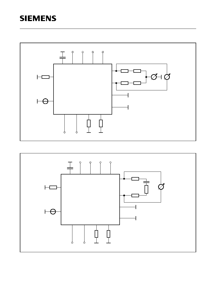
Test Figure 3
Output Current Limit
Test Figure 4
Receive Gain, Transversal Current Ratio, THD, Noise and Power
Supply Rejection
ITS10509
RING
C1
PEB 4065
BIM
V
SS
V
BAT
V
C2
V
2W
PDN
AGND
V
DD
V
H
V
SS
DD
V
V
BAT
H
V
BIM
C
TIP
BGND
See Testcond.
25 k
a
V
a, max
b, max
IL
R
R
IT
V
b
T
L
a
V V
b
,
: BGND /
BAT
V
in PDN, CONV
BGND in BB, RING
ITS10510
TIP
C1
PEB 4065
BIM
V
SS
V
BAT
V
C2
V
2W
PDN
AGND
V
DD
V
H
V
SS
DD
V
V
BAT
H
V
BIM
C
RING
BGND
See Testcond.
25 k
IL
R
R
IT
DC and AC
2W, DC
V
V
2W, AC
V
IT, AC
S
R
R
S
L
R
V
ab, AC
r
G =
ab, AC
V
V
2W, AC
IT, AC
V
V
ab, AC
=
G
IT
1000
660
T
L

PEB/F 4065
Electrical Characteristics
Semiconductor Group
26
1998-03-01
Test Figure 5
Teletax Distortion
Test Figure 6
Longitudinal to Transversal Rejection Ratio
ITS10511
TIP
C1
PEB 4065
BIM
V
SS
V
BAT
V
C2
V
2W
PDN
AGND
V
DD
V
H
V
SS
DD
V
V
BAT
H
V
BIM
C
RING
BGND
See Testcond.
25 k
IL
R
R
IT
2W, DC
V
V
2W, AC
S
R
R
S
L
R
V
ab, AC
2
µ
F
T
L
ITS10512
TIP
C1
PEB 4065
BIM
V
SS
V
BAT
V
C2
V
2W
PDN
AGND
V
DD
V
H
V
SS
DD
V
V
BAT
H
V
BIM
C
RING
BGND
See Testcond.
25 k
IL
R
R
IT
2W, DC
V
V
IT
S
R
R
S
V
ab, AC
R
L/2
L/2
R
~
~
Long
V
T
L
PEB/F 4065
Electrical Characteristics
Semiconductor Group
27
1998-03-01
Test Figure 7
Transversal to Longitudinal Rejection Ratio
Test Figure 8
Ringing
ITS10513
TIP
C1
PEB 4065
BIM
V
SS
V
BAT
V
C2
V
2W
PDN
AGND
V
DD
V
H
V
SS
DD
V
V
BAT
H
V
BIM
C
RING
BGND
See Testcond.
25 k
IL
R
R
IT
2W, DC
V
S
R
R
S
V
ab, AC
R
L/2
L/2
R
Long, AC
V
V
2W, AC
T
L
ITS10514
TIP
C1
PEB 4065
BIM
V
SS
V
BAT
V
C2
V
2W
PDN
AGND
V
DD
V
H
V
SS
DD
V
V
BAT
H
V
BIM
C
RING
BGND
See Testcond.
25 k
IL
R
R
IT
2W
V
S
R
R
S
V
RING
L
R
C
L
T
L

PEB/F 4065
Electrical Characteristics
Semiconductor Group
28
1998-03-01
Test Figure 9
Output Resistance in PDNR Mode
Test Figure 10
TIP, RING Overvoltage Pulses
ITS10515
TIP
C1
PEB 4065
BIM
V
SS
V
BAT
V
C2
V
2W
PDN
AGND
V
DD
IL
R
R
IT
V
H
V
SS
DD
V
V
BAT
H
V
BIM
C
SS
H
BAT
DD
RING
BGND
PDN
R
V
DD
PDN
See Testcond.
TIP
V
RING
V
V
BAT
b
a
V
BAT
T
L
ITS10516
TIP
C1
PEB 4065
BIM
V
SS
V
BAT
V
C2
V
2W
PDN
AGND
V
DD
IL
R
R
IT
V
H
V
SS
DD
V
V
BAT
H
V
V
BIM
BIM
C
SS
H
BAT
DD
RING
BGND
PDN
R
V
REF
V
DD
PDN
30
30
H
V +10 V / 1 ms
+20 V / 1 s
V
H
BAT
V
-10 V / 1 ms
-20 V / 1 s
V
BAT
µ
T
L
µ

PEB/F 4065
Package Outlines
Semiconductor Group
29
1998-03-01
3
Package Outlines
P-DSO-20-5
(Plastic Dual Small Outline Package)
GP
S
0
575
5
Sorts of Packing
Package outlines for tubes, trays etc. are contained in our
Data Book "Package Information".
Dimensions in mm
SMD = Surface Mounted Device