Semiconductor Group 1 1.96
∑
4 194 304 words by 4-bit organization
∑
0 to 70 ∞C operating temperature
∑
Performance:
∑
Single + 3.3 V (± 0.3V ) supply
∑
Low power dissipation
max. 396 active mW (HYB3117400BJ/BT-50)
max. 363 active mW (HYB3117400BJ/BT-60)
max. 330 active mW (HYB3117400BJ/BT-70)
max. 360 active mW (HYB3116400BJ/BT-50)
max. 324 active mW (HYB3116400BJ/BT-60)
max. 288 active mW (HYB3116400BJ/BT-70)
7.2 mW standby (LV-TTL)
3.6 mW standby (LV-CMOS)
720
µ
W standby for L-version
∑
Output unlatched at cycle end allows two-dimensional chip selection
∑
Read, write, read-modify-write, CAS-before-RAS refresh, RAS-only refresh, hidden refresh,
Self Refresh and test mode
∑
Fast page mode capability
∑
All inputs, outputs and clocks fully TTL-compatible
∑
2048 refresh cycles / 32 ms for HYB3117400
4096 refresh cycles / 64 ms for HYB3116400
∑
Plastic Package:
P-SOJ-26/24-1 (300 mil)
P-TSOPII-26/24-1 (300mil)
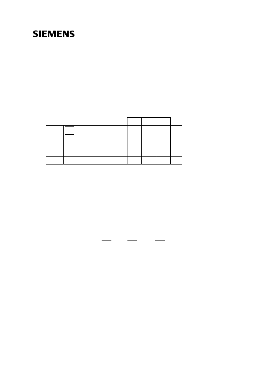
-50
-60
-70
t
RAC
RAS access time
50
60
70
ns
t
CAC
CAS access time
13
15
20
ns
t
AA
Access time from address
25
30
35
ns
t
RC
Read/Write cycle time
90
110
130
ns
t
PC
Fast page mode cycle time
35
40
45
ns
3.3V 4M x 4-Bit Dynamic RAM
Advanced Information
HYB3116400BJ/BT(L) -50/-60/-70
HYB3117400BJ/BT(L) -50/-60/-70

Semiconductor Group
2
HYB 3116(7)400BJ/BT(L) -50/-60/-70
3.3V 4Mx4-DRAM
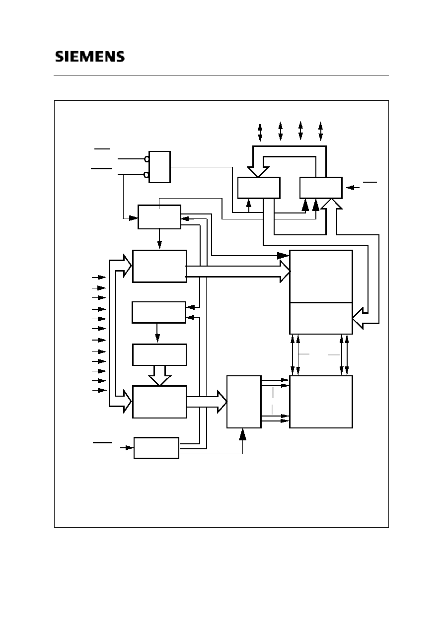
The HYB 3116(7)400BJ/BT is a 16MBit dynamic RAM organized as 4194304 words by 4-bits. The
HYB 3116(7)400BJ/BT utilizes a submicron CMOS silicon gate process technology, as well as
advanced circuit techniques to provide wide operating margins, both internally and for the system
user. Multiplexed address inputs permit the HYB 3116(7)400BJ/BT to be packaged in a standard
SOJ 26/24 300 mil or TSOPII-26/24 300 mil wide plastic package. These packages provide high
system bit densities and are compatible with commonly used automatic testing and insertion
equipment. System-oriented features include single + 3.3 V (± 0.3 V) power supply, direct
interfacing with high-performance logic device families.The HYB3116400BTL parts have a very low
power ,,sleep mode" supported by Self Refresh.
Ordering Information
Type
Ordering Code
Package
Descriptions
HYB 3117400BJ-50
P-SOJ-26/24-1 300 mil
DRAM (access time 50 ns)
HYB 3117400BJ-60
P-SOJ-26/24-1 300 mil
DRAM (access time 60 ns)
HYB 3117400BJ-70
P-SOJ-26/24-1 300 mil
DRAM (access time 70 ns)
HYB 3117400BT-50
P-TSOPII-26/24-1 300 mil
DRAM (access time 50 ns)
HYB 3117400BT-60
P-TSOPII-26/24-1 300 mil
DRAM (access time 60 ns)
HYB 3117400BT-70
P-TSOPII-26/24-1 300 mil
DRAM (access time 70 ns)
HYB 3116400BJ-50
P-SOJ-26/24-1 300 mil
DRAM (access time 50 ns)
HYB 3116400BJ-60
P-SOJ-26/24-1 300 mil
DRAM (access time 60 ns)
HYB 3116400BJ-70
P-SOJ-26/24-1 300 mil
DRAM (access time 70 ns)
HYB 3116400BT-50
P-TSOPII-26/24-1 300 mil
DRAM (access time 50 ns)
HYB 3116400BT-60
P-TSOPII-26/24-1 300 mil
DRAM (access time 60 ns)
HYB 3116400BT-70
P-TSOPII-26/24-1 300 mil
DRAM (access time 70 ns)
HYB 3116400BTL-50
P-TSOPII-26/24-1 300 mil
LP-DRAM (access time 50 ns)
HYB 3116400BTL-60
P-TSOPII-26/24-1 300 mil
LP-DRAM (access time 60 ns)
HYB 3116400BTL-70
P-TSOPII-26/24-1 300 mil
LP-DRAM (access time 70 ns)

Semiconductor Group
3
HYB 3116(7)400BJ/BT(L) -50/-60/-70
3.3V 4Mx4-DRAM
Pin Configuration
Pin Names
A0 to A10
Row & Column Address Inputs for HYB3117400
A0 to A11
Row Address Inputs for HYB3116400
A0 to A9
Column Address Inputs for HYB3116400
RAS
Row Address Strobe
OE
Output Enable
I/O1 -I/O4
Data Input/Output
CAS
Column Address Strobe
WE
Read/Write Input
V
CC
Power Supply (+ 3.3 V)
V
SS
Ground (0 V)
N.C.
not connected
P-SOJ-26/24-1 (300mil)
P-TSOPII-26/24-1 (300mil)
Vcc
I/O1
I/O2
WE
RAS
N.C.
A10
A0
A1
A2
A3
VCC
1
2
3
4
5
6
8
9
10
11
12
13
26
25
24
23
22
21
19
18
17
16
15
14
Vss
I/O4
I/O3
CAS
OE
A9
A8
A7
A6
A5
A4
Vss
HYB3117400BJ/BT
Vcc
I/O1
I/O2
WE
RAS
A11
A10
A0
A1
A2
A3
VCC
1
2
3
4
5
6
8
9
10
11
12
13
26
25
24
23
22
21
19
18
17
16
15
14
Vss
I/O4
I/O3
CAS
OE
A9
A8
A7
A6
A5
A4
Vss
HYB3116400BJ/BT