
Semiconductor Group
31
∑
4 194 304 words by 16-bit organization
∑
0 to 70 ∞C operating temperature
∑
Fast access and cycle time
RAS access time:
50 ns (-50 version)
60 ns (-60 version)
Cycle time:
84 ns (-50 version)
104 ns (-60 version)
CAS access time:
13 ns ( -50 version)
15 ns ( -60 version)
∑
Hyper page mode (EDO) cycle time
20 ns (-50 version)
25 ns (-60 version)
∑
Single + 3.3 V (
±
0.3V) power supply
∑
Low power dissipation
max. 396 active mW ( HYB 3164165T(L)-50)
max. 360 active mW ( HYB 3164165T(L)-60)
max. 504 active mW ( HYB 3165165T(L)-50)
max. 432 active mW ( HYB 3165165T(L)-60)
7.2 mW standby (TTL)
720 W standby (MOS)
14.4 mW Self Refresh (L-version only)
∑
Read, write, read-modify-write, CAS-before-RAS refresh (CBR),
RAS-only refresh, hidden refresh and self refresh modes
∑
Hyper page mode (EDO) capability
∑
2 CAS / 1 WE byte control
∑
8192 refresh cycles/128 ms , 13 R/ 9C addresses (HYB 3164165T(L))
∑
4096 refresh cycles/ 64 ms , 12 R/ 10C addresses (HYB 3165165T(L))
∑
Plastic Package:
P-TSOPII-54-1 500 mil HYB 3164(5)165T(L)
HYB 3164165T(L) -50/-60
HYB 3165165T(L) -50/-60
4M x 16-Bit Dynamic RAM
(4k & 8k Refresh, EDO-version)
Preliminary Information

Semiconductor Group
32
HYB3164(5)165T(L)-50/-60
4M x 16 EDO-DRAM
This HYB3164(5)165 is a 64 MBit dynamic RAM organized 4 194 304 x 16 bits. The device is
fabricated in SIEMENS/IBM most advanced first generation 64Mbit CMOS silicon gate process
technology. The circuit and process design allow this device to achieve high performance and low
power dissipation. The HYB3164(5)165 operates with a single 3.3 +/-0.3V power supply and
interfaces with either LVTTL or LVCMOS levels. Multiplexed address inputs permit the
HYB3164(5)165 to be packaged in a 500mil wide TSOPII-54 plastic package. These packages
provide high system bit densities and are compatible with commonly used automatic testing and
insertion equipment.The HYB3164(5)165TL parts have a very low power ,,sleep mode" supported
by Self Refresh.
Ordering Information
Pin Names
Type
Ordering
Code
Package
Descriptions
HYB 3164165T-50
on request
P-TSOPII-54-1 500 mil
EDO-DRAM (access time 50 ns)
HYB 3164165T-60
on request
P-TSOPII-54-1 500 mil
EDO-DRAM (access time 60 ns)
HYB 3164165TL-50
on request
P-TSOPII-54-1 500 mil
EDO-DRAM (access time 50 ns)
HYB 3164165TL-60
on request
P-TSOPII-54-1 500 mil
EDO-DRAM (access time 60 ns)
HYB 3165165T-50
on request
P-TSOPII-54-1 500 mil
EDO-DRAM (access time 50 ns)
HYB 3165165T-60
on request
P-TSOPII-54-1 500 mil
EDO-DRAM (access time 60 ns)
HYB 3165165TL-50
on request
P-TSOPII-54-1 500 mil
EDO-DRAM (access time 50 ns)
HYB 3165165TL-60
on request
P-TSOPII-54-1 500 mil
EDO-DRAM (access time 60 ns)
A0-A12
Address Inputs for HYB 3164165T(L)
A0-A11
Address Inputs for HYB 3165165T(L)
RAS
Row Address Strobe
OE
Output Enable
I/O1-I/O16
Data Input/Output
UCAS, LCAS
Column Address Strobe
WRITE
Read/Write Input
Vcc
Power Supply ( + 3.3V)
Vss
Ground

Semiconductor Group
33
HYB3164(5)165T(L)-50/-60
4M x 16 EDO-DRAM
Pin Configuration
P-TSOPII-54-1 (500 mil)
* Pin 35 is A12 for HYB 3164165T(L) and N.C. for HYB 3165165T(L)
Semiconductor Group
34
HYB3164(5)165T(L)-50/-60
4M x 16 EDO-DRAM
TRUTH TABLE
FUNCTION
RAS LCAS UCA
S
WRIT
E
OE
ROW
ADD
COL
ADD
I/O1-
I/O16
Standby
H
H - X
H - X
X
X
X
X
High Impedance
Read:Word
L
L
H
H
L
ROW
COL
Data Out
Read:Lower Byte
L
L
H
H
L
ROW
COL
Lower Byte:Data Out
Upper-Byte:High-Z
Read:Upper Byte
L
H
L
H
L
ROW
COL
Lower Byte:High-Z
Upper Byte:Data Out
Write:Word
(Early-Write)
L
L
L
L
X
ROW
COL
Data In
Write:Lower Byte
(Early-Write)
L
L
H
L
X
ROW
COL
Lower Byte:Data Out
Upper-Byte:High-Z
Write:Upper Byte
(Early Write)
L
H
L
L
X
ROW
COL
Lower Byte:High-Z
Upper Byte:Data Out
Read-Modify-
Write
L
L
L
H - L
L - H ROW
COL
Data Out, Data In
Hyper Page Mode
Read (Word)
1st
Cycle
L
H - L
H - L
H
L
ROW
COL
Data Out
Hyper Page Mode
Read (Word)
2nd
Cycle
L
H - L
H - L
H
L
n/a
COL
Data Out
Hyper Page Mode
Early Write(Word)
1st
Cycle
L
H - L
H - L
L
X
ROW
COL
Data In
Hyper Page Mode
Early Write(Word)
2nd
Cycle
L
H - L
H - L
L
X
n/a
COL
Data In
Hyper Page Mode
RMW
1st
Cycle
L
H - L
H - L
H - L
L - H ROW
COL
Data Out, Data In
Hyper Page Mode
RMW
2st
Cycle
L
H - L
H - L
H - L
L - H n/a
COL
Data Out, Data In
RAS only refresh
L
H
H
X
X
ROW
n/a
High Impedance
CAS-before-RAS
refresh
H - L L
L
H
X
X
n/a
High Impedance
Test Mode Entry
H - L L
L
L
X
X
n/a
High Impedance
Hidden Refresh
(Read)
L-H-
L
L
L
H
L
ROW
COL
Data Out
Hidden Refresh
(Write)
L-H-
L
L
L
L
X
ROW
COL
Data In
Self Refresh
(L-version only)
H-L
L
H
X
X
X
X
High Impedance
Semiconductor Group
35
HYB3164(5)165T(L)-50/-60
4M x 16 EDO-DRAM
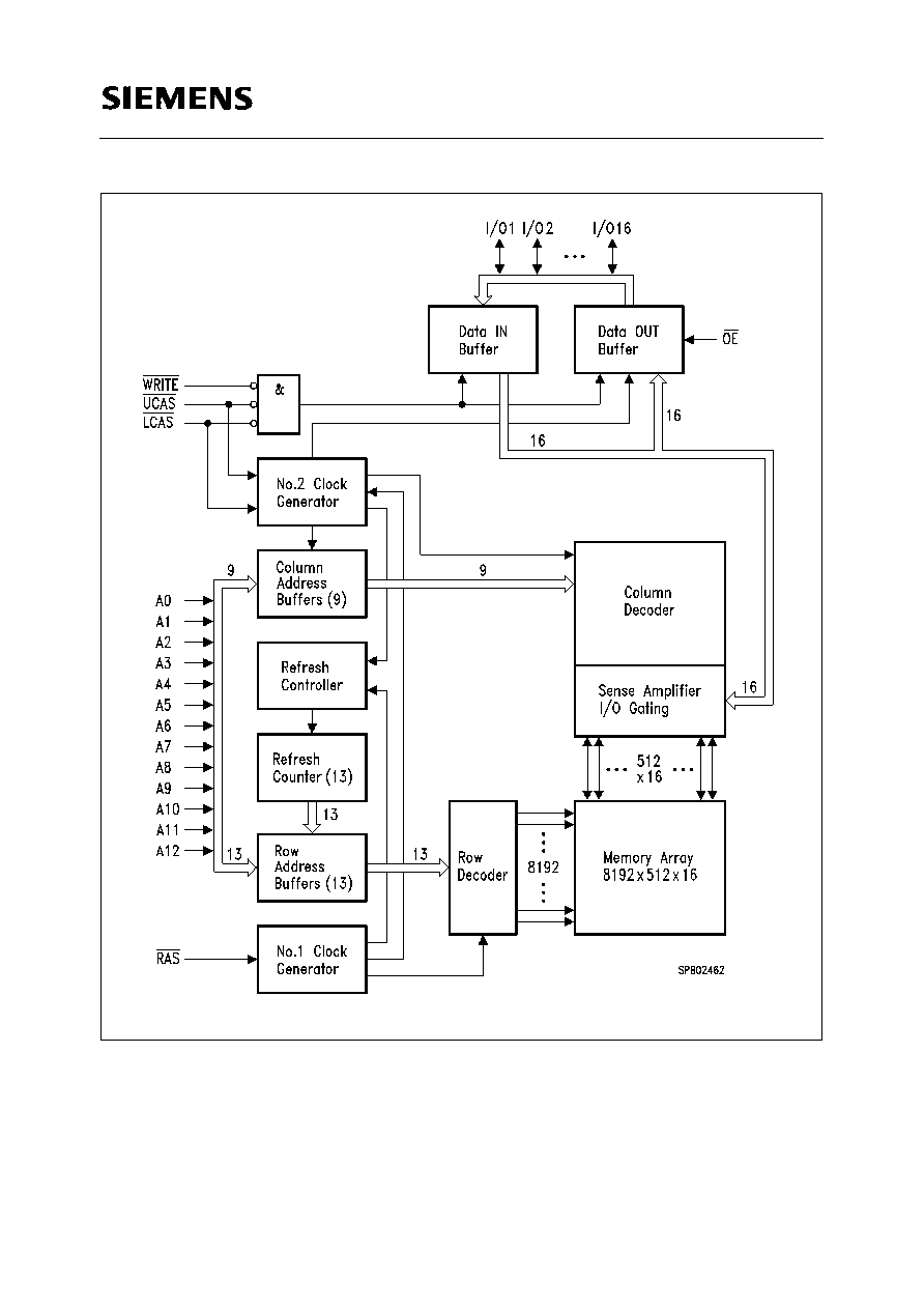
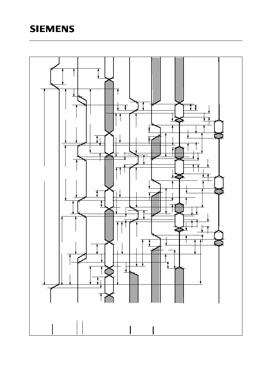
Block Diagram for HYB 3164165T(L)

Semiconductor Group
36
HYB3164(5)165T(L)-50/-60
4M x 16 EDO-DRAM
Block Diagram for HYB 3165165T(L)

Semiconductor Group
37
HYB3164(5)165T(L)-50/-60
4M x 16 EDO-DRAM
Absolute Maximum Ratings
Operating temperature range..............................................................................................0 to 70 ∞C
Storage temperature range.........................................................................................≠ 55 to 150 ∞C
Input/output voltage..................................................................................-0.5 to min (Vcc+0.5,4.6) V
Power supply voltage....................................................................................................-0.5V to 4.6 V
Power dissipation......................................................................................................................1.0 W
Data out current (short circuit)..................................................................................................50 mA
Note
Stresses above those listed under ,,Absolute Maximum Ratings" may cause permanent damage of
the device. Exposure to absolute maximum rating conditions for extended periods may effect device
reliability.
DC Characteristics
T
A
= 0 to 70 ∞C,
V
SS
= 0 V,
V
CC
= 3.3 V
±
0.3 V, (values in brackets for HYB 3165165J/T)
Parameter
Symbol
Limit Values
Unit Note
min.
max.
Input high voltage
V
IH
2.0
Vcc+0.3
V
1)
Input low voltage
V
IL
≠ 0.3
0.8
V
1)
Output high voltage (LVTTL)
Output ,,H" level voltage (Iout = -2mA)
V
OH
2.4
≠
V
Output low voltage (LVTTL)
Output ,,L"level voltage (Iout = +2mA)
V
OL
≠
0.4
V
Output high voltage (LVCMOS)
Output ,,H" level voltage (Iout = -100uA)
V
OH
Vcc-0.2 -
V
Ouput low voltage (LVCMOS)
Output ,,L" level voltage (Iout = +100uA)
V
OL
-
0.2
V
Input leakage current,any input
(0 V < Vin < Vcc , all other pins = 0 V
I
I(L)
≠ 2
2
µ
A
Output leakage current
(DO is disabled, 0 V < Vout < Vcc )
I
O(L)
≠ 2
2
µ
A
Average Vcc supply current:
-50 ns version
-60 ns version
(RAS, CAS, address cycling: tRC = tRC min.)
I
CC1
≠
≠
110 (140)
100 (120)
mA
mA
2) 3) 4)
Standby Vcc supply current
(RAS=CAS= Vih)
I
CC2
≠
2
mA
≠
Semiconductor Group
38
HYB3164(5)165T(L)-50/-60
4M x 16 EDO-DRAM
Average Vcc supply current, during RAS-only
refresh cycles:
-50 ns version
-60 ns version
(RAS cycling: CAS = VIH: tRC = tRC min.)
I
CC3
≠
≠
110 (140)
100 (120)
mA
mA
2) 4)
Average Vcc supply current,
Hyper page mode (EDO):
-50 ns version
-60 ns version
(RAS =
V
IL
, CAS, address cycling: tHPC=tHPC min.)
I
CC4
≠
≠
115 (150)
100 (120)
mA
mA
2) 3) 4)
Standby Vcc supply current
(RAS=CAS= Vcc-0.2V)
I
CC5
≠
200
A
≠
Average Vcc supply current, during CAS-before-
RAS refresh mode:
-50 ns version
-60 ns version
(RAS, CAS cycling: tRC = tRC min.)
I
CC6
≠
≠
110 (140)
100 (120)
mA
mA
2) 4)
Self Refresh Current (L-version only)
Average Power Supply Current during Self Refresh.
(CBR cycle with tRAS>TRASSmin, CAS held low,
WE = Vcc-0.2V, Address and Din=Vcc-0.2V or 0.2V)
I
CC7
≠
400
A
Capacitance
T
A
= 0 to 70 ∞C,
V
CC
= 3.3 V
±
0.3 V,
f
= 1 MHz
Parameter
Symbol
Limit Values
Unit
min.
max.
Input capacitance (A0 to A11,A12)
C
I1
≠
5
pF
Input capacitance (RAS, CAS, WRITE, OE)
C
I2
≠
7
pF
I/O capacitance (I/O1-I/O16)
C
IO
≠
7
pF
DC Characteristics
(cont'd)
T
A
= 0 to 70 ∞C,
V
SS
= 0 V,
V
CC
= 3.3 V
±
0.3 V, (values in brackets for HYB 3165165J/T)
Parameter
Symbol
Limit Values
Unit Note
min.
max.

Semiconductor Group
39
HYB3164(5)165T(L)-50/-60
4M x 16 EDO-DRAM
AC Characteristics
5)6)
T
A
= 0 to 70 ∞C,
V
CC
= 3.3 V
±
0.3V ,
t
T
= 2 ns
Parameter
Symbol
Limit Values
Unit
Note
-50
-60
min.
max.
min.
max.
common parameters
Random read or write cycle time
t
RC
84
≠
104
≠
ns
RAS precharge time
t
RP
30
≠
40
≠
ns
RAS pulse width
t
RAS
50
100k
60
100k
ns
CAS pulse width
t
CAS
8
10k
10
10k
ns
Row address setup time
t
ASR
0
≠
0
≠
ns
Row address hold time
t
RAH
8
≠
10
≠
ns
Column address setup time
t
ASC
0
≠
0
≠
ns
Column address hold time
t
CAH
8
≠
10
≠
ns
RAS to CAS delay time
t
RCD
12
37
14
45
ns
RAS to column address delay time
t
RAD
10
25
12
30
ns
RAS hold time
t
RSH
8
10
≠
ns
CAS hold time
t
CSH
45
50
≠
ns
CAS to RAS precharge time
t
CRP
5
≠
5
≠
ns
Transition time (rise and fall)
t
T
1
50
1
50
ns
7
Refresh period for HYB3164165
t
REF
≠
128
≠
128
ms
Refresh period for HYB3165165
t
REF
≠
64
≠
64
ms
Read Cycle
Access time from RAS
t
RAC
≠
50
≠
60
ns
8, 9
Access time from CAS
t
CAC
≠
13
≠
15
ns
8, 9
Access time from column address
t
AA
≠
25
≠
30
ns
8,10
OE access time
t
OEA
≠
13
≠
15
ns
Column address to RAS lead time
t
RAL
25
≠
30
≠
ns
Read command setup time
t
RCS
0
≠
0
≠
ns
Read command hold time
t
RCH
0
≠
0
≠
ns
11
Read command hold time referenced to
RAS
t
RRH
0
≠
0
≠
ns
11
CAS to output in low-Z
t
CLZ
0
≠
0
≠
ns
8
Semiconductor Group
40
HYB3164(5)165T(L)-50/-60
4M x 16 EDO-DRAM
Output buffer turn-off delay
t
OFF
0
13
0
15
ns
12
Output buffer turn-off delay from OE
t
OEZ
0
13
0
15
ns
12
Data to CAS low delay
t
DZC
0
≠
0
≠
ns
13
Data to OE low delay
t
DZO
0
≠
0
≠
ns
13
CAS high to data delay
t
CDD
13
≠
15
≠
ns
14
OE high to data delay
t
ODD
13
≠
15
≠
ns
14
Write Cycle
Write command hold time
t
WCH
8
≠
10
≠
ns
Write command pulse width
t
WP
7
≠
10
≠
ns
Write command setup time
t
WCS
0
≠
0
≠
ns
15
Write command to RAS lead time
t
RWL
8
≠
10
≠
ns
Write command to CAS lead time
t
CWL
8
≠
10
≠
ns
Data setup time
t
DS
0
≠
0
≠
ns
16
Data hold time
t
DH
7
≠
10
≠
ns
16
Read-modify-Write Cycle
Read-write cycle time
t
RWC
111
≠
135
≠
ns
RAS to WE delay time
t
RWD
67
≠
79
≠
ns
15
CAS to WE delay time
t
CWD
30
≠
34
≠
ns
15
Column address to WE delay time
t
AWD
42
≠
49
≠
ns
15
OE command hold time
t
OEH
7
≠
10
≠
ns
Hyper Page Mode (EDO) Cycle
Hyper page mode (EDO) cycle time
t
HPC
20
≠
25
≠
ns
CAS precharge time
t
CP
8
≠
10
≠
ns
Access time from CAS precharge
t
CPA
≠
27
≠
35
ns
7
Output data hold time
t
COH
5
≠
5
≠
ns
RAS pulse width in hyper page mode
t
RAS
50
200k
60
200k
ns
CAS precharge to RAS Delay
t
RHCP
27
≠
35
≠
ns
AC Characteristics
(cont'd)
5)6)
T
A
= 0 to 70 ∞C,
V
CC
= 3.3 V
±
0.3V ,
t
T
= 2 ns
Parameter
Symbol
Limit Values
Unit
Note
-50
-60
min.
max.
min.
max.

Semiconductor Group
41
HYB3164(5)165T(L)-50/-60
4M x 16 EDO-DRAM
OE pulse width
t
OEP
7
≠
10
≠
ns
OE hold time from CAS high
t
OEHC
7
≠
10
≠
ns
WE pulse width to output disable at CAS
high
t
WPZ
7
≠
10
≠
ns
Output buffer turn-off delay from WE
t
WPZ
0
10
0
10
ns
Hyper Page Mode (EDO) Read-
modify-Write Cycle
Hyper page mode (EDO) read-write
cycle time
t
PRWC
51
≠
66
≠
ns
CAS precharge to WE
t
CPWD
41
≠
49
≠
ns
CAS before RAS refresh cycle
CAS setup time
t
CSR
5
≠
5
≠
ns
CAS hold time
t
CHR
8
≠
10
≠
ns
RAS to CAS precharge time
t
RPC
5
≠
5
≠
ns
Write to RAS precharge time
t
WRP
8
≠
10
≠
ns
Write hold time referenced to RAS
t
WRH
8
≠
10
≠
ns
CAS-before-RAS counter test cycle
CAS precharge time (CAS-before-RAS
counter test cycle)
t
CPT
35
≠
40
≠
ns
Self Refresh Cycle
RAS pulse width during self refresh
t
RASS
100k
_
100k
_
ns
17
RAS precharge time during self refresh
t
RPS
84
_
104
_
ns
17
CAS hold time during self refresh
t
CHS
-50
_
-50
_
ns
17
AC Characteristics
(cont'd)
5)6)
T
A
= 0 to 70 ∞C,
V
CC
= 3.3 V
±
0.3V ,
t
T
= 2 ns
Parameter
Symbol
Limit Values
Unit
Note
-50
-60
min.
max.
min.
max.

Semiconductor Group
42
HYB3164(5)165T(L)-50/-60
4M x 16 EDO-DRAM
Notes:
1) All voltages are referenced to VSS.
Vih may overshoot to VV + 0.2V for pulse widths of < 4ns with 3.3V. Vil may undershoot to -2.0V for pulse width
< 4.0 ns with 3.3V. Pulse width measured at 50% points with amplitude measured peak to DC reference.
2) ICC1, ICC3, ICC4 and ICC6 and ICC7 depend on cycle rate.
3) ICC1 and ICC4 depend on output loading. Specified values are measured with the output open.
4) Address can be changed once or less while RAS = Vil.In the case of ICC4 it can be changed once or less
during a Hyper page mode cycle ( thpc).
5) An initial pause of 100 s is required after power-up followed by 8 RAS-only-refresh cycles, before proper
device operation is achieved. In case of using internal refresh counter, a minimum of 8 CAS-before-RAS
initialization cycles instead of 8 RAS cycles are required.
6) AC measurements assume tT = 2 ns.
7) VIH (min.) and VIL (max.) are reference levels for measuring timing of input signals. Also, transition times are
measured between VIH and VIL.
8) Measured with the specified current load and 100 pF at Voh = 2.0 V and Vol = 0.8 V.
9) Operation within the tRCD (max.) limit ensures that tRAC (max.) can be met. tRCD (max.) is specified as a
reference point only: If tRCD is greater than the specified tRCD (max.) limit, then access time is controlled by
tCAC.
10) Operation within the tRAD (max.) limit ensures that tRAC (max.) can be met. tRAD (max.) is specified as a
reference point only: If tRAD is greater than the specified tRAD (max.) limit, then access time is controlled by
tAA.
11) Either tRCH or tRRH must be satisfied for a read cycle.
12) tOFF (max.) and tOEZ (max.) define the time at which the outputs achieve the open-circuit condition and are
not referenced to output voltage levels.
13) Either tDZC or tDZO must be satisfied.
14) Either tCDD or tODD must be satisfied.
15) tWCS, tRWD, tCWD, tAWD and tCPWD are not restrictive operating parameters. They are included in the data
sheet as electrical characteristics only. If tWCS > tWCS (min.), the cycle is an early write cycle and the I/O pin
will remain open-circuit (high impedance) through the entire cycle; if tRWD > tRWD (min.), tCWD > tCWD
(min.), tAWD > tAWD (min.) and tCPWD > tCPWD (min.) , the cycle is a read-write cycle and I/O pins will
contain data read from the selected cells. If neither of the above sets of conditions is satisfied, the condition
of the I/O pins (at access time) is indeterminate.
16) These parameters are referenced to CAS leading edge in early write cycles and to WRITE leading edge in
Read-Modify-Write cycles.
17) When using Self Refresh mode, the following refresh operations must be performed to ensure proper DRAM
operation:
If row addresses are being refresh in an evenly distributed manner over the refresh interval using CBR refresh
cycles, then only one CBR cycle must be performed immediatly after exit from Self Refresh.
If row addresses are being refresh in any other manner (ROR - Distributed/Burst or CBR-Burst) over the
refresh interval, then a full set of row refreshed must be performed immediately before entry to and immediatey
after exit from Self Refresh
Semiconductor Group
43
HYB3164(5)165T(L)-50/-60
4M x 16 EDO-DRAM
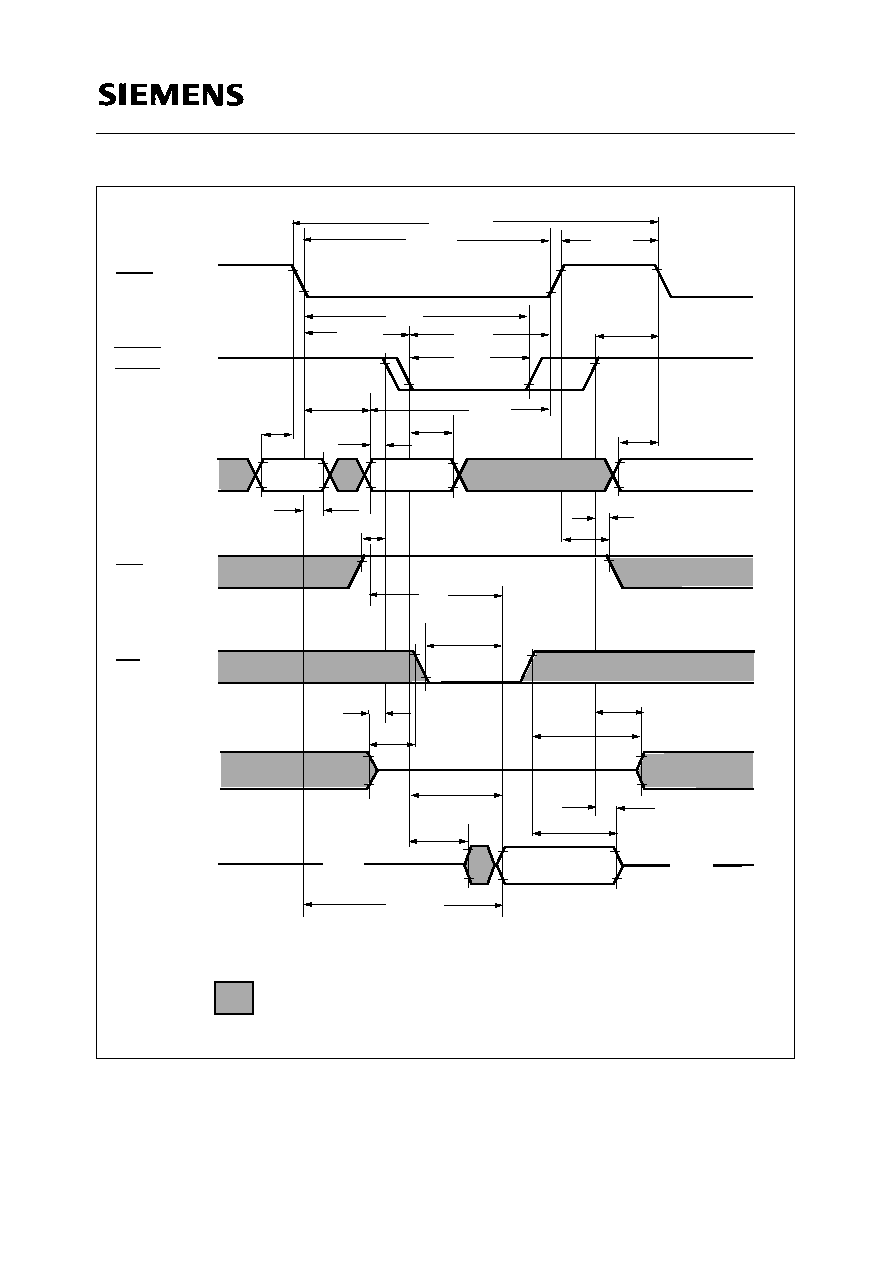
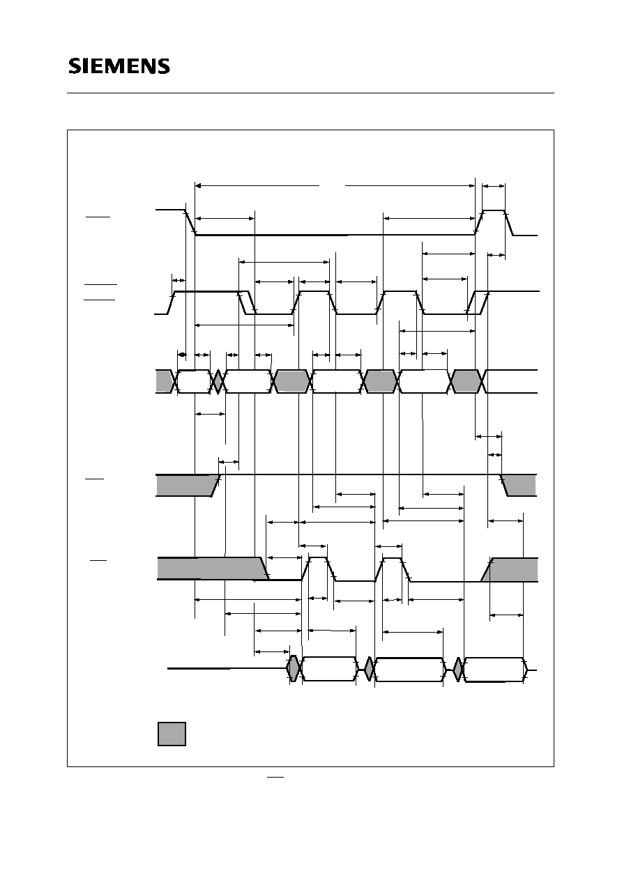
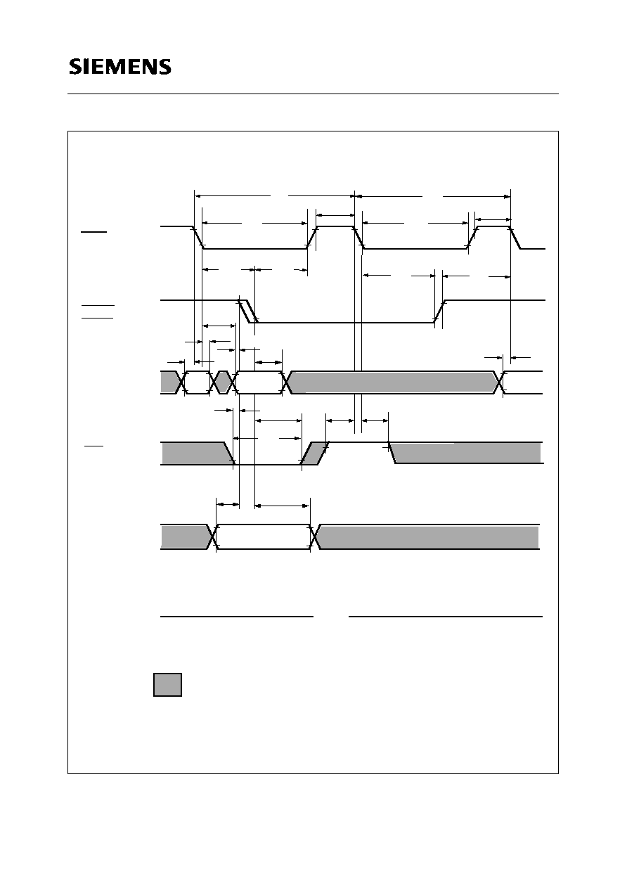
Read Cycle
Row
Column
Row
Valid Data Out
RAS
UCAS
Address
WE
OE
I/O
(Inputs)
I/O
(Outputs)
V
IH
V
IL
V
IH
V
IL
V
IH
V
IL
V
IH
V
IL
V
IH
V
IL
V
IH
V
IL
V
OH
V
OL
t
RAS
t
RC
t
CSH
t
RAD
t
CAS
t
RP
t
RAH
t
CRP
t
RSH
t
RCD
t
RAL
t
ASR
t
CAH
t
ASC
t
ASR
t
RCH
t
RRH
t
RCS
t
AA
t
OEA
t
CLZ
t
CAC
t
OEZ
t
ODD
t
CDD
t
OFF
t
DZC
t
DZO
t
RAC
Hi Z
Hi Z
"H" or "L"
WL1
LCAS
Semiconductor Group
44
HYB3164(5)165T(L)-50/-60
4M x 16 EDO-DRAM
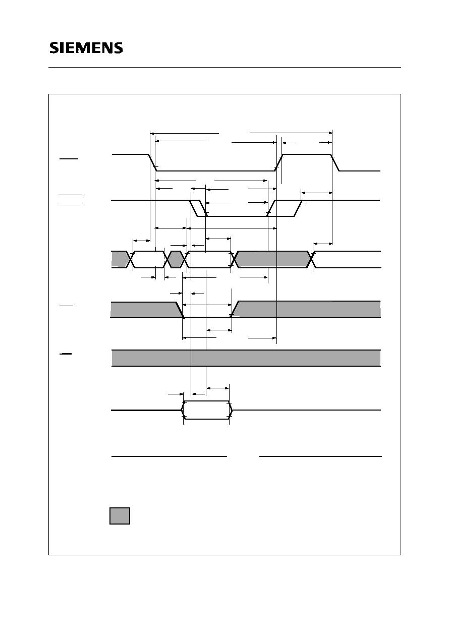
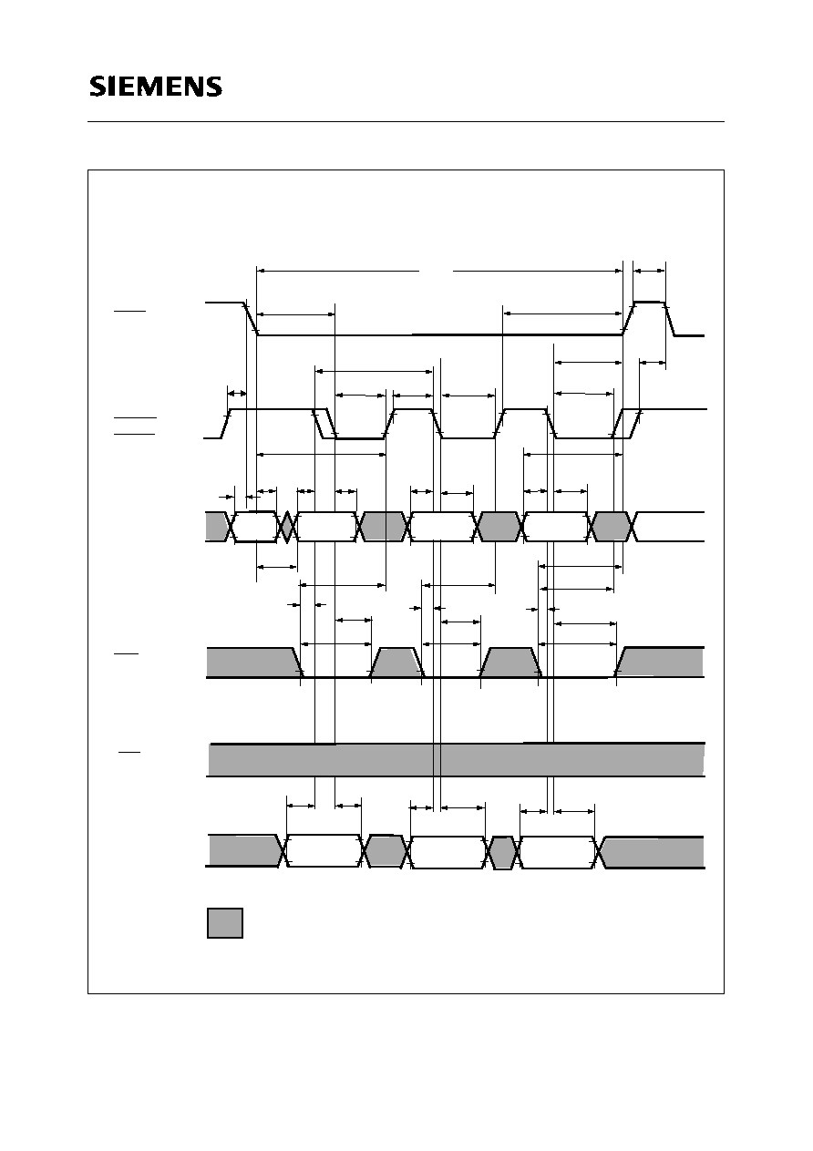
Write Cycle (Early Write)
RAS
UCAS
Address
WE
OE
I/O
(Inputs)
I/O
(Outputs)
V
IH
V
IL
V
IH
V
IL
V
IH
V
IL
V
IH
V
IL
V
IH
V
IL
V
IH
V
IL
V
OH
V
OL
.
t
RAS
t
RC
t
CSH
t
RAD
t
CAS
t
RP
t
CRP
t
RSH
t
RCD
t
RAL
t
ASR
t
CAH
t
ASR
t
CWL
t
RWL
t
WP
t
ASC
t
WCH
Valid Data In
t
DS
t
DH
Hi Z
Column
Row
Row
t
RAH
t
WCS
"H" or "L"
WL2
LCAS

Semiconductor Group
45
HYB3164(5)165T(L)-50/-60
4M x 16 EDO-DRAM
Write Cycle (OE Controlled Write)
Valid Data
t
RWL
t
WP
t
OEH
t
ODD
t
CWL
t
DZO
t
OEA
t
CLZ
t
DS
t
OEZ
t
DH
t
RC
V
IH
V
IL
Row
t
DZC
"H" or "L"
Hi-Z
Hi-Z
Column
Row
t
ASC
t
RAD
t
RAL
t
CAH
t
RAH
RAS
UCAS
Address
WE
OE
I/O
(Inputs)
I/O
(Outputs)
V
IH
V
IL
V
IH
V
IL
V
IH
V
IL
V
IH
V
IL
V
IH
V
IL
V
OH
V
OL
.
t
RAS
t
CSH
t
CAS
t
RP
t
CRP
t
RSH
t
RCD
t
ASR
t
ASR
WL3
LCAS
Semiconductor Group
46
HYB3164(5)165T(L)-50/-60
4M x 16 EDO-DRAM
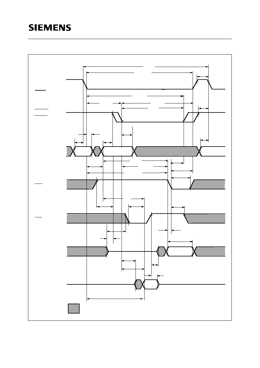
Read-Write (Read-Modify-Write) Cycle
Row
Row
t
CSH
t
CAS
t
CRP
t
RWC
t
AWD
t
ASR
t
RP
t
RAS
t
RAH
t
CAH
I/O
(Outputs)
V
OH
V
OL
V
IH
V
IL
V
IH
V
IL
I/O
(Inputs)
OE
WE
V
IH
V
IL
t
ASR
Column
t
RCD
t
DH
t
RSH
t
RAD
t
CWD
t
OEH
t
RWD
t
RWL
t
CWL
t
CLZ
t
WP
t
RCS
t
AA
t
OEA
t
DS
t
DZC
t
DZO
t
ODD
t
CAC
t
OEZ
Valid
Data in
Data
Out
t
RAC
"H" or "L"
t
ASC
V
IH
V
IL
V
IH
V
IL
RAS
UCAS
Address
V
IH
V
IL
WL4
LCAS
Semiconductor Group
47
HYB3164(5)165T(L)-50/-60
4M x 16 EDO-DRAM
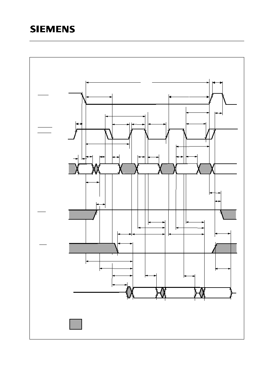
Hyper Page Mode (EDO) Read Cycle
t
RP
t
RSH
t
CAS
t
CAS
t
CP
t
CRP
t
RAL
t
CAH
t
CAH
t
ASC
t
CSH
t
CAS
t
RCD
t
RAH
t
ASR
Column 2
Row
Data Out
RAS
I/O
WE
Address
UCAS
V
IH
V
IL
V
IH
V
IL
V
IH
V
IL
VIH
V
IL
V
IH
V
IL
"H" or "L"
V
OH
V
OL
OE
t
RAS
t
CRP
t
ASC
t
HPC
t
CAH
t
RAD
t
RHCP
t
ASC
t
RCS
t
RRH
t
RCH
(Output)
t
RAC
t
AA
t
CAC
t
CLZ
t
OEA
t
OES
t
COH
t
CAC
t
AA
t
CPA
Data Out
Column N
Column 1
Data Out
t
OEZ
t
OFF
t
CAC
t
AA
t
CPA
1
2
t
COH
N
WL5
LCAS
Semiconductor Group
48
HYB3164(5)165T(L)-50/-60
4M x 16 EDO-DRAM
Hyper Page Mode (EDO) Read Cycle (OE Control)
LCAS
t
RP
t
RSH
t
CAS
t
CAS
t
CP
t
CRP
t
RAL
t
CAH
t
CAH
t
ASC
t
CSH
t
CAS
t
RCD
t
RAH
t
ASR
Column 2
Row
Data Out
RAS
I/O
WE
Address
UCAS
V
IH
V
IL
V
IH
V
IL
V
IH
V
IL
VIH
V
IL
V
IH
V
IL
"H" or "L"
V
OH
V
OL
OE
t
RAS
t
CRP
t
ASC
t
HPC
t
CAH
t
RAD
t
RHCP
t
ASC
t
RCS
t
RRH
t
RCH
(Output)
t
RAC
t
AA
t
CAC
t
CLZ
t
OEA
t
OES
t
OEZ
t
CAC
t
AA
t
CPA
Data Out
Column N
Column 1
Data Out
t
OEZ
t
OFF
t
CAC
t
AA
t
CPA
1
2
N
t
OEP
t
OEHC
t
OEA
t
OEP
t
OEHC
t
OEZ
t
OEA
WL6

Semiconductor Group
49
HYB3164(5)165T(L)-50/-60
4M x 16 EDO-DRAM
Hyper Page Mode (EDO) Read Cycle (WE Control)
t
RP
t
RSH
t
CAS
t
CAS
t
CP
t
CRP
t
RAL
t
CAH
t
CAH
t
ASC
t
CSH
t
CAS
t
RCD
t
RAH
t
ASR
Column 2
Row
Data Out
RAS
I/O
WE
Address
UCAS
V
IH
V
IL
V
IH
V
IL
V
IH
V
IL
VIH
V
IL
V
IH
V
IL
"H" or "L"
V
OH
V
OL
OE
t
RAS
t
CRP
t
ASC
t
HPC
t
CAH
t
RAD
t
RHCP
t
ASC
t
RCS
t
RRH
t
RCH
(Output)
t
RAC
t
AA
t
CAC
t
CLZ
t
OEA
t
OES
t
WHZ
t
CAC
t
AA
t
CPA
Data Out
Column N
Column 1
Data Out
t
OEZ
t
OFF
t
CAC
t
AA
t
CPA
1
2
N
t
RCH
t
RCS
t
WPZ
t
RCH
t
RCS
t
WPZ
t
WHZ
WL7
LCAS
Semiconductor Group
50
HYB3164(5)165T(L)-50/-60
4M x 16 EDO-DRAM
Hyper Page Mode (EDO) Early Write Cycle
t
RP
t
RSH
t
CAS
t
CAS
t
CP
t
CRP
t
RAL
t
CAH
t
CAH
t
ASC
t
CWL
t
WCS
t
WP
t
WCH
t
CSH
t
CAS
t
RCD
t
RAH
t
ASR
t
DH
t
DS
t
DH
t
DS
Column 1
Column 2
Row
Addr
Data In N
Data In 2
Data In 1
Column N
RAS
I/O (Input)
WE
Address
UCAS
V
IH
V
IL
V
IH
V
IL
V
IH
V
IL
VIH
V
IL
V
IH
V
IL
"H" or "L"
V
OH
V
OL
OE
t
RAS
t
CRP
t
ASC
t
CWL
t
WCS
t
WP
t
WCH
t
CWL
t
WCS
t
WP
t
WCH
t
RWL
t
DH
t
DS
t
HPC
t
CAH
t
RAD
t
RHCP
t
ASC
WL8
LCAS

Semiconductor Group
51
HYB3164(5)165T(L)-50/-60
4M x 16 EDO-DRAM
Hyper Page Mode (EDO) Late Write Cycle
t
RP
t
RSH
t
CAS
t
CAS
t
CP
t
CRP
t
RAL
t
CAH
t
CAH
t
ASC
t
CSH
t
CAS
t
RCD
t
RAH
t
ASR
Column 2
Row
Data In
RAS
I/O
WE
Address
UCAS
V
IH
V
IL
V
IH
V
IL
V
IH
V
IL
VIH
V
IL
V
IH
V
IL
"H" or "L"
V
OH
V
OL
OE
t
RAS
t
CRP
t
ASC
t
HPC
t
CAH
t
RAD
t
ASC
t
RCS
(Input)
t
ODD
t
DH
Data In
Column N
Column 1
Data In
t
OEH
1
2
N
t
WP
t
RCS
t
WP
WL16
CP
t
t
DS
t
DH
t
DS
t
WP
t
DS
t
DH
t
RCS
t
CWL
t
CWL
t
CWL
t
RWL
t
ODD
t
OEH
t
ODD
t
OEH
LCAS
Semiconductor Group
52
HYB3164(5)165T(L)-50/-60
4M x 16 EDO-DRAM
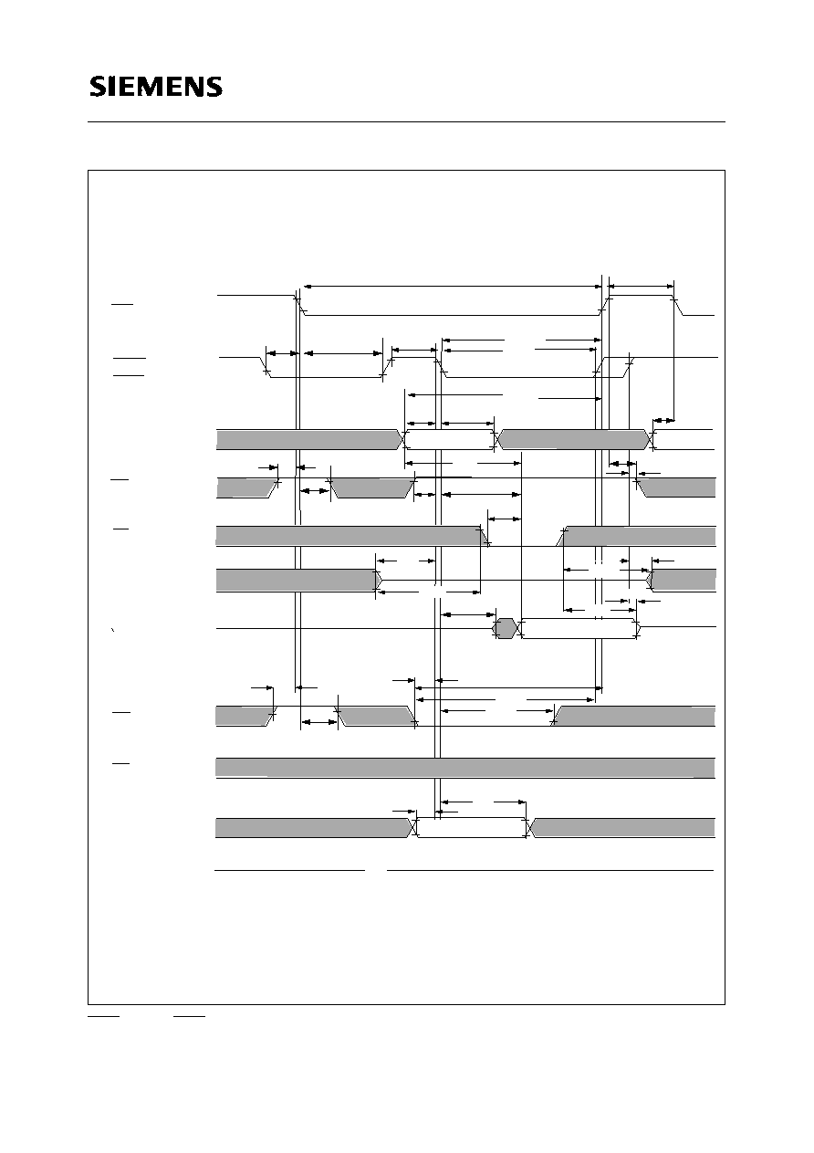
Hyper Page Mode (EDO) Read-Modify-Write Cycle
t
CAH
t
CP
t
DZC
t
DZO
t
RAC
t
CAC
t
CLZ
t
RCS
t
AA
t
OEA
t
RCD
t
RAD
t
RAH
t
ASR
t
ASC
t
CAS
t
CAS
t
PRWC
t
CWD
t
CAH
t
ASC
t
CAS
t
RSH
t
RP
t
CRP
t
ASR
t
CAH
t
ASC
t
RAL
t
CWD
t
RWD
t
CWL
t
CWL
t
CWD
t
AWD
t
AWD
t
WP
t
WP
t
CWL
t
RWL
t
AWD
t
WP
t
ODD
t
OEH
t
DH
t
DS
t
CPA
t
OEZ
t
CLZ
t
DZC
t
AA
t
CAC
t
OEA
t
DS
t
OEZ
t
DH
t
OEH
t
AA
t
ODD
t
DZC
t
CPA
t
OEA
t
CLZ
t
DS
t
DH
t
OEH
t
ODD
RAS
V
IH
V
IL
UCAS
V
IH
V
IL
V
IH
V
IL
V
IH
V
IL
V
IH
V
IL
V
IH
V
IL
V
OH
V OL
WE
OE
Address
I/O
(Inputs)
I/O
(Outputs)
Data In
Data In
Data In
Data
Out
Out
Data
Data Out
Row
Column
Column
Row
t
RASP
t
CSH
Column
t
CPWD
t
CPWD
WL17
LCAS

Semiconductor Group
53
HYB3164(5)165T(L)-50/-60
4M x 16 EDO-DRAM
RAS Only Refresh Cycle
t
CRP
t
RAH
t
RP
t
RAS
t
RC
t
ASR
t
ASR
t
RPC
V
IH
V
IL
V
IH
V
IL
V
IH
V
IL
V
OH
V
OL
Row
Row
HI-Z
Address
RAS
UCAS
I/O
(Outputs)
"H" or "L"
WL9
LCAS

Semiconductor Group
54
HYB3164(5)165T(L)-50/-60
4M x 16 EDO-DRAM
CAS-before-RAS Refresh Cycle
t
RP
t
RAS
t
RP
t
RC
t
CRP
t
CP
t
RPC
t
CHR
t
WRH
t
WRP
t
CSR
t
RPC
t
OFF
t
OEZ
t
CDD
t
ODD
V
IH
V
IL
V
IH
V
IL
V
IH
V
IL
V
IH
V
IL
V
IH
V
IL
HI-Z
"H" or "L"
RAS
I/O
(Outputs)
I/O
(Inputs)
OE
WE
UCAS
V
OH
V
OL
WL10
LCAS
Semiconductor Group
55
HYB3164(5)165T(L)-50/-60
4M x 16 EDO-DRAM
Hidden Refresh Read Cycle
RAS
I/O
(Outputs)
I/O
(Inputs)
OE
WE
Address
UCAS
t
RC
t
RC
t
RAS
t
RAS
t
RP
t
RP
t
CRP
t
CHR
t
RAD
t
CAH
t
ASC
t
RAH
t
ASR
t
ASR
t
RCS
t
RRH
t
AA
t
DZC
t
DZO
t
CAC
t
RAC
t
CLZ
t
OEZ
t
OFF
t
ODD
t
CDD
t
RCD
t
RSH
t
OEA
V
IH
V
IL
V
IH
V
IL
V
IH
V
IL
V
IH
V
IL
V
IH
V
IL
V
IH
V
IL
t
WRP
t
WRH
"H" or "L"
Valid Data Out
Row
Column
Row
HI-Z
V
OH
V
OL
WL11
LCAS
Semiconductor Group
56
HYB3164(5)165T(L)-50/-60
4M x 16 EDO-DRAM
Hidden Refresh Early Write Cycle
RAS
I/O
(Output)
I/O
(Input)
WE
Address
V
IH
V
IL
V
IH
V
IL
V
IH
V
IL
UCAS
V
IH
V
IL
V
IH
V
IL
"H" or "L"
t
RC
t
RAS
t
RCD
t
RSH
t
RAD
t
CAH
t
WCS
t
WCH
t
WP
t
ASR
t
RAH
t
DS
t
DH
t
ASR
t
CRP
t
CHR
t
RP
t
RAS
t
RC
t
RP
t
ASC
Row
Row
Valid Data
HI-Z
Column
V
OH
V
OL
t
WRP
t
WRH
WL12
LCAS
Semiconductor Group
57
HYB3164(5)165T(L)-50/-60
4M x 16 EDO-DRAM
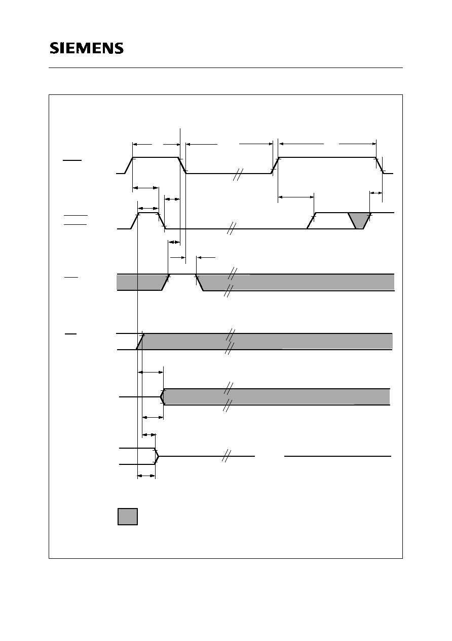
Self Refresh (Sleep Mode)
t
RPS
t
RASS
t
RP
t
CRP
t
CP
t
RPC
t
WRH
t
WRP
t
CSR
t
OFF
t
OEZ
t
CDD
t
ODD
V
IH
V
IL
V
IH
V
IL
V
IH
V
IL
V
IH
V
IL
V
IH
V
IL
HI-Z
"H" or "L"
RAS
I/O
(Outputs)
I/O
(Inputs)
OE
WE
UCAS
V
OH
V
OL
t
CHS
WL13
LCAS
Semiconductor Group
58
HYB3164(5)165T(L)-50/-60
4M x 16 EDO-DRAM
CAS-before-RAS Refresh Counter Test Cycle
t
CSR
t
ASR
t
ASC
t
CHR
t
CP
t
WRP
t
RAL
t
CAH
t
RSH
t
RP
t
RAS
t
CAS
t
RCS
t
CDD
t
CAC
t
AA
t
WRH
t
OEA
t
ODD
t
CLZ
t
DZC
t
DZO
t
OEZ
t
OFF
t
RWL
t
CWL
t
WCH
t
WCS
t
WRH
t
WRP
t
DS
t
DH
V
IH
V
IL
V
IH
V IL
V
IH
V IL
VOH
VOL
V
IH
V IL
V
IH
V IL
V
IH
V IL
V
IH
V IL
V
IH
V IL
V
IH
V IL
V
IH
V IL
RAS
I/O
(Inputs)
OE
WE
Address
UCAS
I/O
(Outputs)
I/O
(Outputs)
I/O
(Inputs)
WE
OE
Column
Row
Data Out
Data In
HI-Z
Read Cycle:
Write Cycle:
t
RRH
t
RCH
LCAS
Semiconductor Group
59
HYB3164(5)165T(L)-50/-60
4M x 16 EDO-DRAM
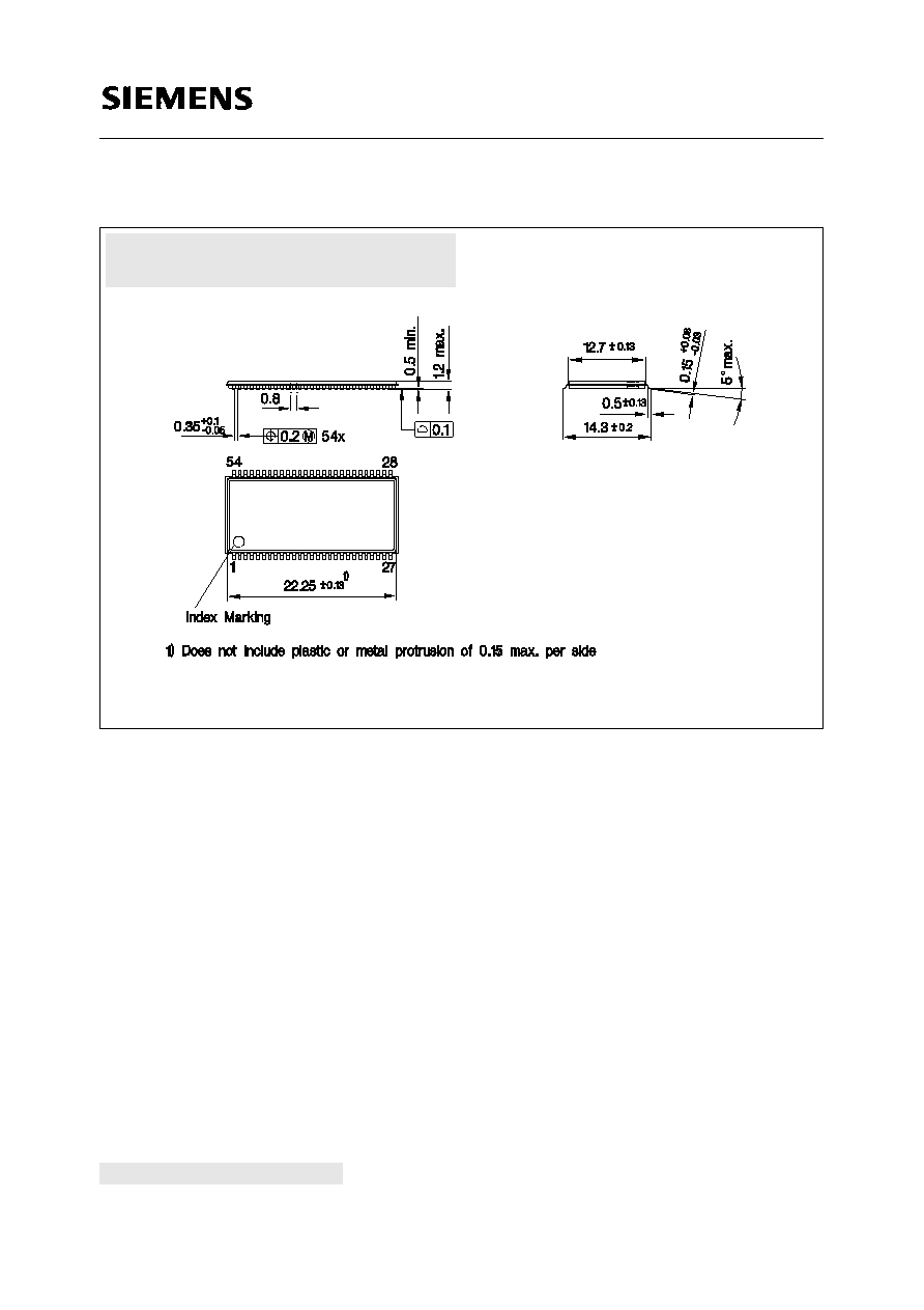
Package Outlines
P-TSOPII-54-1 (500 mil)
(Plastic Thin Small Outline Package Type II
Sorts of Packing
Package outlines for tubes, trays etc. are contained in our
Data Book "Package Information".
Dimensions in mm
SMD = Surface Mounted Device

((60))
VAKAT