
Semiconductor Group
1
1998-10-01
Overview
The HYB 39S163200TQ are dual bank Synchronous Graphics DRAM's (SGRAM) organized as
2 banks
�
256 Kbit
�
32 with built-in graphics features. These synchronous devices achieve high
speed data transfer rates up to 143 MHz by employing a chip architecture that prefetches multiple
bits and then synchronizes the output data to a system clock. The chip is fabricated with an
advanced 64MBit DRAM process technology.
The device is designed to comply with all JEDEC standards set for synchronous graphics DRAM
products, both electrically and mechanically.
RAS, CAS, WE, DSF and CS are pulsed signals which are examined at the positive edge of each
externally applied clock. Internal chip operating modes are defined by combinations of these
signals. A ten bit address bus accepts address data in the conventional RAS/CAS multiplexing
style. Ten row address bits (A0 - A9) and a bank select BA are strobed with RAS. Column address
bits plus a bank select are strobed with CAS.
Prior to any access operation, the CAS latency, burst length and burst sequence must be
programmed into the device by address inputs during a mode register set cycle. An Auto Precharge
function may be enabled to provide a self-timed row precharge. This is initiated at the end of the
burst sequence. In addition, it features the write per bit, the block write and the masked block write
� High Performance:
� Single Pulsed RAS Interface
� Programmable CAS Latency: 2, 3
� Fully Synchronous to Positive Clock Edge
� Programmable Wrap Sequence:
Sequential or Interleave
� Programmable Burst Length:
1, 2, 4, 8 and full page for sequential
1, 2, 4, 8 for interleave
-6
-7
-7
-8
Units
f
CK
166
125
125
125
MHz
latency
3
2
3
3
-
t
CK3
6
8
7
8
ns
t
AC3
5.5
5.5
5.5
6
ns
� Special Mode Registers
� Two color registers
� Burst Read with Single Write Operation
� Block Write and Write-per-Bit Capability
� Byte controlled by DQM0-3
� Auto Precharge and Auto Refresh Modes
� Suspend Mode and Power Down Mode
� 2k refresh cycles/32 ms
�
t
AC
= 5 ns
�
t
SETUP
/
t
HOLD
= 2 ns/1 ns
� Latency 2 @ 125 MHz
� Random Column Address every CLK
(1-N Rule)
� Single 3.3 V
�
0.3 V Power Supply
� LVTTL compatible inputs and outputs
HYB 39S13620TQ-6/-7/-8
HYB 39S16320TQ-6/-7/-8
Semiconductor Group
2
1998-10-01
functions. By having a programmable Mode register and Special Mode register, the system can
select the best suitable modes to maximize its performance.
Operating the two memory banks in an interleave fashion allows random access operation to occur
at higher rate than is possible with standard DRAMs. A sequential and gapless data rate of up to
143 MHz is possible depending on burst length, CAS latency and speed grade of the device.
Auto Refresh (CBR) and Self Refresh operation are supported.
These devices operate with a single 3.3 V
�
0.3 V power supply and are available in 100 pin TQFP
package.
Features
� All signals fully synchronous to the positiv edge of the system clock
� Programmable burst lengths: 1, 2, 4, 8 or full page
� Burst data transfer in sequential or interleaved order
� Burst read with single write
� Programmable CAS latency: 2, 3
� 8 column block write and write-per-bit modes
� Independent byte operation via DQM 0
...
3 interface
� Auto precharge and auto refresh modes
� 2k refresh cycles/32 ms
� LVTTL compatible I/O
� Hidden auto precharge for read bursts
Ordering Information
Type
Ordering Code
Package
Description
SDR LVTTL-Version
HYB 39S16320TQ-6
on request
TQFP-100-1
256k
�
2
�
32 SGRAM
HYB 39S16320TQ-7
on request
TQFP-100-1
256k
�
2
�
32 SGRAM
HYB 39S16320TQ-8
on request
TQFP-100-1
256k
�
2
�
32 SGRAM
HYB 39S16320TQ-10
on request
TQFP-100-1
256k
�
2
�
32 SGRAM

HYB 39S16320TQ-6/-7/-8
Semiconductor Group
3
1998-10-01
Pin Configuration
100 pin TQFP
DQ28
V
DDQ
DQ25
DQ24
D15
D12
D13
D14
DQ11
V
DDQ
DQ9
DQM3
DQM1
MCH
DQ8
N.C.
A8 / AP
CKE
DSF
CLK
DQ0
DQ2
DQ1
V
DQ29
N.C.
WE
CAS
A9
RAS
DQM2
DQM0
DQ4
DQ18
DQ23
DQ22
DQ21
DQ20
DQ19
DQ16
DQ7
DQ6
DQ5
DQ3
A2
N.C.
A7
A6
A5
A4
N.C.
N.C.
N.C.
N.C.
N.C.
N.C.
N.C.
N.C.
N.C.
A3
A1
A0
85
90
95
100
50
40
35
45
1
5
10
15
20
25
30
55
60
65
70
75
80
SPP03942
SS
DDQ
V
SSQ
V
DDQ
V
DQ17
SSQ
V
DDQ
V
DD
V
SS
V
SSQ
V
DDQ
V
CS
BA
V
DD
SS
V
SSQ
V
DQ10
DD
V
SS
V
DDQ
V
SSQ
V
DDQ
V
SSQ
V
DQ27
DQ26
V
SSQ
DQ30
DQ31
N.C.
N.C.
N.C.
N.C.
N.C.
N.C.
N.C.
N.C.
N.C.
DD
V
V
SSQ
20
�
14 mm
2
0.65 mm pitch
(Marking side)

HYB 39S16320TQ-6/-7/-8
Semiconductor Group
4
1998-10-01
Pin Definitions and Functions
CLK
Clock Input
DQ0 to DQ31
DataInput/Output
CKE
Clock Enable
DQM0 to DQM3 Data Mask
CS
Chip Select
V
DD
Power (+ 3.3 V)
RAS
Row Address Strobe
V
SS
Ground
CAS
Column Address Strobe
V
DDQ
Power for DQ's (+ 3.3 V)
WE
Write Enable
V
SSQ
Ground for DQ's
A0 - A9
Address Inputs
NC
Not connected
A8 - AP
Auto Precharge
DSF
Special Function Enable
BA
Bank Select
MCH
Must Connect High

HYB 39S16320TQ-6/-7/-8
Semiconductor Group
5
1998-10-01
Signal Pin Description
Pin
Type
Signal Polarity Function
CLK
Input
Pulse
Positive
Edge
The system clock input. All of the SGRAM inputs are
sampled on the rising edge of the clock.
CKE
Input
Level
Active
High
Activates the CLK signal when high and deactivates the
CLK signal when low. By deactivating the clock, CKE low
initiates the Power Down mode, Suspend mode, or the Self
Refresh mode.
CS
Input
Pulse
Active
Low
CS enables the command decoder when low and disables
the command decoder when high. When the command
decoder is disabled, new commands are ignored but
previous operations continue.
RAS
CAS
WE
Input
Pulse
Active
Low
When sampled at the positive rising edge of the clock,
CAS, RAS, and WE define the operation to be executed by
the SGRAM.
A0 - A9
Input
Level
�
During a Bank Activate command cycle, A0-A9 defines the
row address (RA0-RA9) when sampled at the rising clock
edge.
During a Read or Write command cycle, A0-A7 defines the
column address (CA0-CA7) when sampled at the rising
clock edge.
In addition to the column address, CA8 is used to invoke
autoprecharge operation at the end of the burst read or
write cycle. If A8 is high, autoprecharge is selected and BA
defines the bank to be precharged (low = bank A,
high bank B). If A8 is low, autoprecharge is disabled.
During a Precharge command cycle, A8 is used in
conjunction with BA to control which bank(s) to precharge.
If A8 is high, both bank A and bank B will be precharged
regardless of the state of BA. If A8 is low, then BA is used
to define which bank to precharge.
BA
Input
Level
�
Selects which bank is activated. BA low selects bank A and
BA high selects bank B.
DQ0 -
DQ31
Input
Output
Level
�
Data Input/Output pins operate in the same manner as on
conventional DRAMs, with the exception of the Block Write
function. In this case, the DQx pins perform a masking
operation.

HYB 39S16320TQ-6/-7/-8
Semiconductor Group
6
1998-10-01
DQM0 -
DQM3
Input
Pulse
�
During Read, DQM = 1 turns off the output buffers.
During Write, DQM = 1 prevents a write to the current
memory location.
DQM0 corresponds to DQ0 - DQ7
DQM1 corresponds to DQ8 - DQ15
DQM2 corresponds to DQ16 - DQ23
DQM3 corresponds to DQ24 - DQ31
V
DD
V
SS
Supply �
�
Power and ground for the input buffers and the core logic.
V
DDQ
V
SSQ
Supply �
�
Isolated power supply and ground for the output buffers to
provide improved noise immunity.
DSF
Input
Level
�
DSF is part of the input command to the SGRAM. If DSF is
low, SGRAM operates in the same way as SDRAMs. When
DSF is high it enables the block write and masked write
and special mode register setup cycle.
Signal Pin Description
(cont'd)
Pin
Type
Signal Polarity Function

HYB 39S16320TQ-6/-7/-8
Semiconductor Group
7
1998-10-01
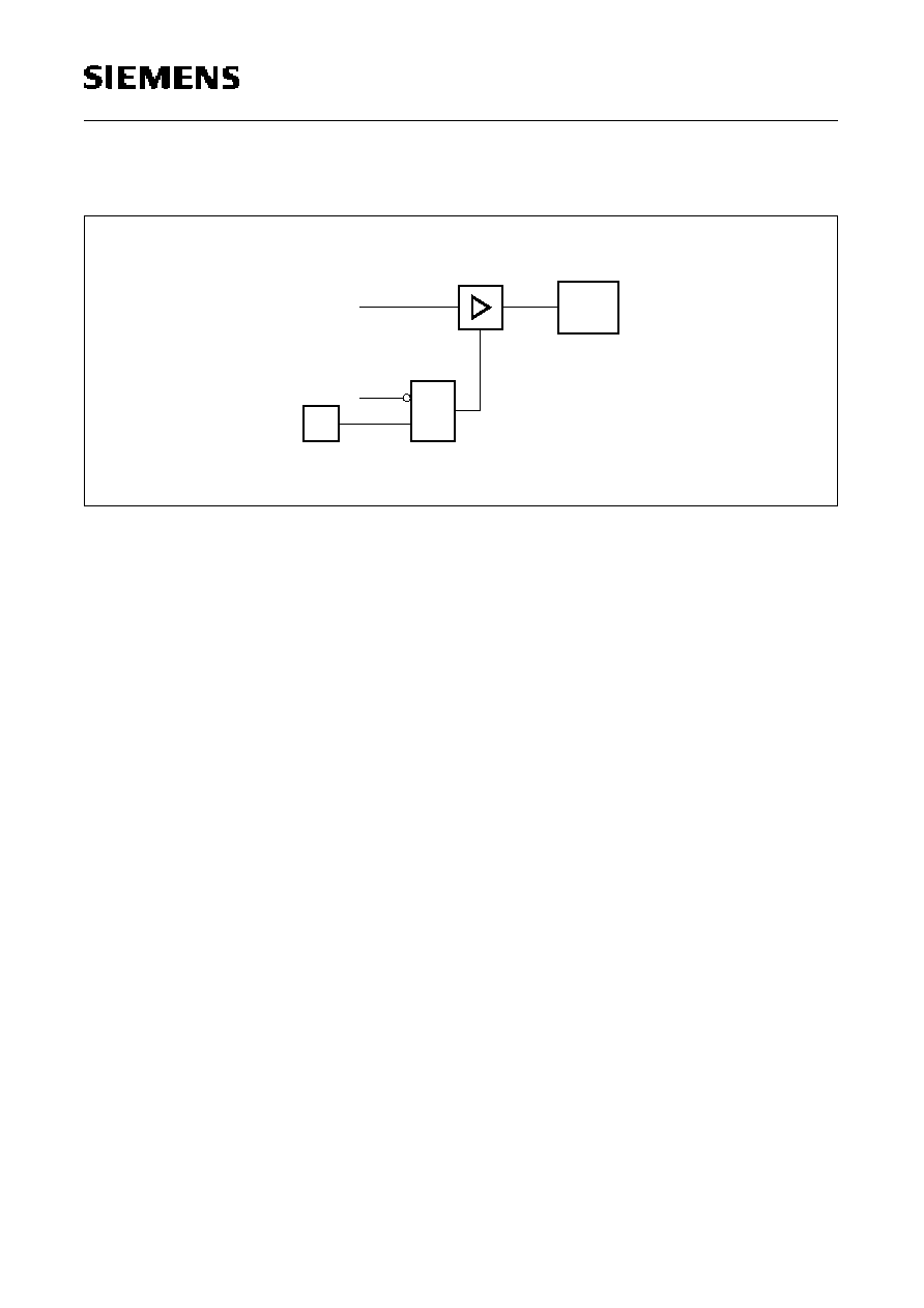
Functional Block Diagrams
A0 - A7,
AP, BA
Column Addresses
Address Buffer
Column
Address Counter
Column
A0 - A9,
BA
Row Addresses
Row Address
Buffer
Counter
Refresh
Sense Amplifier & I(O) Bus
Column Decoder
Bank 1
1024 x
Row
Decoder
Array
Memory
Sense Amplifier & I(O) Bus
Column Decoder
Bank 0
1024 x
Row
Decoder
Array
Memory
Input Buffer
Output Buffer
DQ0 - DQ31
Control Logic & Timing Generator
DQMx DSF CLK CKE CS RAS CAS
SPB03936
256 x
32 Bit
256 x
32 Bit
WE
Color Register
Mask Register

HYB 39S16320TQ-6/-7/-8
Semiconductor Group
8
1998-10-01
Functional Description
General
The 16 Mbyte SGRAM is a dual bank 1024
�
256
�
32 DRAM with graphics features of Block Write
and Masked Write. It consists of two banks. Each bank is organized as 1024
rows
�
256 columns
�
32 bits.
Read and Write accesses are burst oriented. Accesses begin with the registration of an Activate
command which is then followed by a Read or Write command. The address bits registered
coincident with the Active command are used to select the bank and the row to be accessed. BA
selects the bank and address bits A9 - A0 select the row. Address bits A7 - A0 registered coincident
with the Read or Write command are used to select the starting column location for the burst
access.
Block Writes are not burst oriented and always apply to eight column locations selected by A7 - A3.
DQs registered at Block Write command are used to mask the selected columns. DQs registered
coincident with the Load Special Mode Register command are used as Color Data (LC-Bit = 1) or
Persistent Mask (LM = 1). If LC and LM are both 1 in the same Load Special Mode Register
command cycle, the data of the Mask and the Color Register will be unknown.
Initialization
The default power on state of the mode register is supplier specific and may be undefined. The
following power on and initialization sequence guarantees, that the device is preconditioned to each
users specific needs.
The following sequence is recommended:
� During power on, all
V
DD
and
V
DDQ
pins must be built up simultaneously to the specified voltage
when the input signals are held in the "NOP" state.
� The power on voltage must not exceed
V
DD
+ 0.3 V on any of the input pins or
V
DD
supplies.
� The CLK signal must be started at the same time.
� After power on, an initial pause of 200
�
s is required.
� The pause is followed by a precharge of both banks using the precharge command.
� To prevent data contention on the DQ bus during power on, it is required that the DQM and
CKE pins be held high during the initial pause period.
� Once all banks have been precharged, the Mode Register Set Command must be issued to
initialize the Mode Register.
� A minimum of eight Auto Refresh cycles (CBR) are also required.
It is also possible to reverse the last two steps of the initialization procedure:
First send at least 8 CBR commands, then the LMR command.
Failure to follow these steps may lead to unpredictable start-up modes.

HYB 39S16320TQ-6/-7/-8
Semiconductor Group
9
1998-10-01
Mode Register Programming
The Mode Register is used to define: a Burst Length, a Burst type, a Read Latency and an operating
mode. The mode register is programmed via the Load Mode Register command and will retain the
stored information until it is programmed again or the device looses power. The mode register must
be loaded when both banks are idle and the controller must wait the specified time before initiating
the subsequent command. Violating either of these requirements may result in unknown operation.
Burst Length
Read and Write operations to the SGRAM are burst oriented, with the burst length being
programmable. The burst length determines the maximum number of column locations that can be
accessed for a given Read or Write command. Burst lengths of 1, 2, 4, or 8 locations are available
for both the sequential and the interleaved burst types and a Full Page Burst is available for the
sequential type. The Full Page Burst is used in conjunction with the Burst Terminate command to
generate arbitrary burst lengths.
When a Read or Write command is issued, a block of columns equal to the burst length is selected.
The block is defined by address bits A7 - A1 when the burst length is set to 2, by A7-A2 for burst
length set to 4 and by A7 - A3 for burst length set to 8. The lower order bit(s) are used to select the
starting location within the block. The burst will wrap within the block if a boundary is reached.
Burst Type
Accesses within a given burst may be programmed to be either sequential or interleaved and the
type is selected based on the setting of BT bit in the mode register. If BT is set to "0", the burst type
is sequential, if BT is "1", the burst type is interleave.
Read Latency
The Read Latency is the delay in clock cycles between the registration of a Read command and the
availability of the first piece of output data. The latency can be set to 2 or 3 clocks. If a Read
command is registered at clock edge n and the Read Latency is 2 clocks, the data will be available
by clock edge n + 2. The DQs will start driving already one cycle earlier (n + 1).
Color Register
The Siemens 16M SGRAM offers two Color Registers. If Bit M7 is set to "1", two Color Register
mode is specified.
Operation Mode
In normal operation, the bits M8 and M9 of Mode Register (MR) are set "0". The programmed burst
length applies to both read and write bursts. When bit M8 is set to "1", burst read and single write
mode is selected.
Test modes and reserved states should not be used because unknown operation or incompatibility
with future versions may result.

HYB 39S16320TQ-6/-7/-8
Semiconductor Group
10
1998-10-01
Load Special Mode Register (LSMR)
The Special Mode Register command is used to load the mask and color registers, which are used
in Block Write and Masked Write cycles.The data to be written to either the color registers or the
Mask Register is applied to the DQs and the control information is applied to the address inputs.
During a LSMR cycle, if the address bit A6 is "1", and all other address inputs are "0", the Color
Register 0 will be loaded with the data on the DQs. If the address bits A6 and A7 are both set equal
to "1" and Mode Register M7 bit was already set to "1", Color Register 1 will be loaded with the data
on the DQs.This color data is used for Block Write cycles. Similarly, when input A5 is "1", and all
other address inputs are "0" during a LSMR cycle, the mask register will be loaded with the data on
the DQs. Never Set bit A5 to "1" when A6 and/or A7 are set equal to "1" in the same Load Special
Mode Register cycle to avoid unknown operation.
Color Registers
Two Color Registers (Color Register 0 and Color Register 1) are available in the devices. Each color
register is a 32-bit register which supplies the data during Block Write cycles. The Color Register is
loaded via a Load Special Mode Register command, as shown in the Function Truth table and will
retain data until loaded again with a new data or until power is removed from the SGRAM.
Mask Register
The Mask Register (or the Write-per-Bit mask register) is a 32-bit register which acts as a per-bit
mask during Masked Write and Masked Block Write cycles. The Mask Register is loaded via the
Load Special Mode Register command and will retain data until loaded again or until power is
removed from the SGRAM.

HYB 39S16320TQ-6/-7/-8
Semiconductor Group
11
1998-10-01
Commands
The Function Truth Table provides a quick reference of available commands.
Operation
CKE
n
-
1
CKE
n
CS
RAS
CAS
WE
DSF
DQM
BA
A8
A0 -
A7
Device Deselect
(INHBT)
H
X
H
X
X
X
X
X
X
X
X
No Operation (NOP)
H
X
L
H
H
H
X
X
X
X
X
Load Mode Register
(LMR)
H
X
L
L
L
L
L
X
X
OPCODE
Load Special Mode
Register (LSMR)
H
X
L
L
L
L
H
X
X
OPCODE
Row Activate (ACT)
H
X
L
L
H
H
L
X
BA
Row Addr
Row Active with WpB
(ACTM)
H
X
L
L
H
H
H
X
BA
Row Addr
Read (RD)
H
X
L
H
L
H
X
X
BA
L
Col.
Read with Auto
Precharge (RDA)
H
X
L
H
L
H
X
X
BA
H
Col.
Write Command
(WR)
H
X
L
H
L
L
L
X
BA
L
Col.
Write Command with
Auto Precharge
(WRA)
H
X
L
H
L
L
L
X
BA
H
Col.
Block Write (BW)
H
X
L
H
L
L
H
X
BA
L
Col.
Block Write with Auto
Precharge (BWA)
H
X
L
H
L
L
H
X
BA
H
Col.
Burst Terminate
(BST)
H
X
L
H
H
L
X
X
X
X
X
Precharge Single
Bank (PRE)
H
X
L
L
H
L
X
X
BA
L
X
Precharge All Banks
(PREAL)
H
X
L
L
H
L
X
X
X
H
X
Auto Refresh (REF)
H
H
L
L
L
H
X
X
X
X
X
Self Refresh Entry
(SREF (EN)
H
L
L
L
L
H
X
X
X
X
X
Self Refresh Exit
(SREF (EX)
L
L
H
H
H
L
X
H
X
H
X
H
X
X
X
X
X
X
X
X
X
X
Power Down Mode
Entry (PDN-EN)
H
H
L
L
H
L
X
H
X
H
X
H
X
X
X
X
X
X
X
X
X
X
Power Down Mode
Exit (PDN-EX)
L
H
X
X
X
X
X
X
X
X
X

HYB 39S16320TQ-6/-7/-8
Semiconductor Group
12
1998-10-01
Notes
1. All inputs are latched on the rising edge of the CLK.
2. LMR, REF and SREF commands should be issued only after both banks are deactivated
(PREAL command).
3. ACT and ACTM command should be issued only after the corresponding bank has been
deactivated (PRE command).
4. WR, WRA, RD, RDA should be issued after the corresponding bank has been activated
(ACT command).
5. Auto Precharge command is not valid for full-page burst.
6. BW and BWA commands use mask register data only after ACTM command. DQM byte masking
is active regardless of WPB mask.
7. Loading Mask Register: Initiate an LSMR cycle with address pin A5 = 1 to load the mask register
with the mask data present on DQ pins. Except A5, all other address pins must be "0" during
LSMR cycle while loading the mask register.
8. Loading Color Register: Initiate an LSMR cycle with address pin A6 = 1 to load the color register
with the color input data on DQ pins. Address pin A7 selects color register. Except A6 and A7, all
other address pins must be "0" during LSMR cycle while loading a color register. If one color
register mode is enabled, all address pins, except A6, must be "0" during LSMR cycle.
9. If BW or BWA operation is initiated and 2-Color Register Mode is initialized by the mode register,
address A0 selects the desired color register for the operation. If A0 = 0, color register 0 will be
used, if A0 = 1, color register 1.
10.Any Write or Block Write cycles to the selected bank/row while active will be masked according
to the contents of the mask register, in addition to the DQM signals and the column/byte mask
information (the later for Block Writes only).
11.Block Writes are not burst oriented and always apply to the eight column locations selected by
A7 - A3.
12.Addressline A9 is always "X" with the exception of two commands:
In LMR and LSMR commands it provides opcode (see description Mode and Special Mode
Register). In ACT and ACTM commands it provides the address bit 9 of the row address.

HYB 39S16320TQ-6/-7/-8
Semiconductor Group
13
1998-10-01
Address Input for Mode Set (Mode Register Functions)
A9
A8
A7
A6
A5
A4
A3
A2
A1
A0
Write Mode
CAS Latency
BT
Burst Length
Address Bus (Ax)
Mode Register (Mx)
Operation Mode
M8
M9
Mode
Normal
0
0
Multiple Burst
0
1
Burst Type
M3
Type
Sequential
Interleave
0
1
M6
M5
M4
Latency
CAS Latency
0
0
0
Reserved
0
0
1
Reserved
0
1
0
2
0
1
1
3
1
0
0
Reserved
1
0
1
1
1
0
Reserved
1
1
1
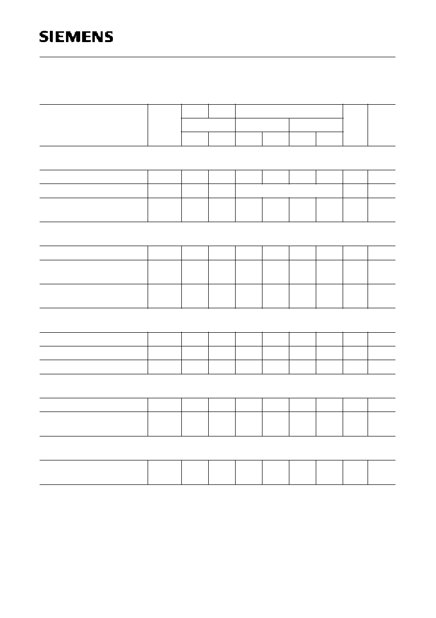
Address Input for Mode Set (Mode Register Functions)
1
1
1
1
0
0
0
0
M2
1
2
0
0
1
1
1
0
0
1
1
0
1
1
1
0
0
M1
0
M0
8
4
Length
Burst Length
Sequential
Interleave
Full Page
1
2
4
8
SPB03935
CR
with Single Write
0
M7
1
Color Register
Two Color register
One Color register
Registers
Reserved
Reserved
Reserved
Reserved
Reserved
Reserved
Reserved
Reserved
Reserved

HYB 39S16320TQ-6/-7/-8
Semiconductor Group
14
1998-10-01
Burst Length and Sequence
Full page Burst
Full Page Burst is an extension of the above tables of sequential addressing with the burst length
being 256.
Burst of two
Starting Address
(Column Address A0)
Sequential Addressing
Sequence (decimal)
Interleave Addressing
Sequence (decimal)
0
0, 1
0, 1
1
1, 0
1, 0
Burst of four
Starting Address
(Column Address A1 - A0)
Sequential Addressing
Sequence (decimal)
Interleave Addressing
Sequence (decimal)
0
0, 1, 2, 3
0, 1, 2, 3
1
1, 2, 3, 0
1, 0, 3, 2
2
2, 3, 0, 1
2, 3, 0, 1
3
3, 0, 1, 2
3, 2, 1, 0
Burst of eight
Starting Address
(Column Address A1 - A0)
Sequential Addressing
Sequence (decimal)
Interleave Addressing
Sequence (decimal)
0
0, 1, 2, 3, 4, 5, 6, 7
0, 1, 2, 3, 4, 5, 6, 7
1
1, 2, 3, 4, 5, 6, 7, 0
1, 0, 3, 2, 5, 4, 7, 6
2
2, 3, 4, 5, 6, 7, 0, 1
2, 3, 0, 1, 6, 7, 4, 5
3
3, 4, 5, 6, 7, 0, 1, 2
3, 2, 1, 0, 7, 6, 5, 4
4
4, 5, 6, 7, 0, 1, 2, 3
4, 5, 6, 7, 0, 1, 2, 3
5
5, 6, 7, 0, 1, 2, 3, 4
5, 4, 7, 6, 1, 0, 3, 2
6
6, 7, 0, 1, 2, 3, 4, 5
6, 7, 4, 5, 2, 3, 0, 1
7
7, 0, 1, 2, 3, 4, 5, 6
7, 6, 5, 4, 3, 2, 1, 0

HYB 39S16320TQ-6/-7/-8
Semiconductor Group
15
1998-10-01
Special Mode Register Functions
Note: If only one Color Register is in use, A7 is Don't Care.
Special Mode Register Naming Conventions
Device Deselect (INHBT)
The device deselect or inhibit function prevents commands from being executed by the SGRAM,
regardless of whether the CLK signal is enabled. The device is effectively deactivated (CS is high).
No Operation (NOP)
The NOP command is used to perform a no operation to an SGRAM which is selected (CS is low).
This prevents unwanted commands being registered during idle or wait states. The execution of the
command(s) already in progress will not be affected.
Load Mode Register (LMR)
The Mode Register is loaded via address input pins A9 - A0 . The LMR command can only be issued
when both banks are idle, and a subsequent executable command can not be issued until 2 CLK
cycle Latency is met.
Load Special Mode Register (LSMR)
LSMR command is used to load either the Color Register(s) or the Mask Register at a time. The
control information is provided on inputs A9 - A0, while the data for the Color or Mask Register is
provided on the DQs. The LSMR command can be issued when both banks are idle, or one or both
are active but with no Read, Write or Block Write accesses in progress.
Address Bits
Functions
A9
A8
A7
A6
A5
A4
A3
A2
A1
A0
0
0
0
0
1
0
0
0
0
0
Load Mask Register
0
0
0
1
0
0
0
0
0
0
Load Color Register 0
0
0
1
1
0
0
0
0
0
0
Load Color Register 1
Address bit name
Special name
Function
A5
LM
Load Mask Enable
A6
LC
Load Color Enable
A7
SCR
Select Color Register

HYB 39S16320TQ-6/-7/-8
Semiconductor Group
16
1998-10-01
Active (ACT)
The ACT command is used to open (or activate) a row in a particular bank. The value on BA selects
the bank and the address provided on input pins A9 - A0 selects the row. This row remains open
for accesses until a Precharge command is issued to the bank. A Precharge command must be
issued before opening a different row in the same bank.
Active with WPB (ACTM)
ACTM command is similar to the ACT command, except that the Write-per-Bit mask is activated.
Any Write or Block Write cycles to the selected bank/row while active will be masked according to
the contents of the Mask Register.
Read (RD)
The Read command is used to initiate a burst read access from an active row. The value on BA
selects the bank and the address provided on inputs A7 - A0 selects the starting column location.
The value on A8 determines whether or not Auto Precharge is used. If A8 is "1", Auto Precharge is
used. If Auto Precharge is selected, the row being accessed will be precharged at the end of the
read burst; if Auto Precharge is not selected, the row will remain open for subsequent accesses. If
a particular DQM was registered high, the corresponding DQs appearing 2 clocks later on the
output pins will be High-Z.
Write (WR)
The Write command is used to initiate a burst write access to an active row. The value on BA selects
the bank and the address provided on inputs A7 -A0 selects the starting column location. The value
on A8 determines whether or not Auto Precharge is used. If A8 is "1", Auto Precharge is used. If
Auto Precharge is selected, the row being accessed will be precharged at the end of write burst; if
Auto Precharge is not selected, the row will remain open for subsequent accesses. If a particular
DQM is registered high, the corresponding data inputs will be ignored and the write will not be
executed to that byte location.
Block Write (BW)
The Block Write command is used to write a single data value to the block of eight consecutive
column locations addressed by inputs A7 - A3 . The data is provided by the Color Register which
must be loaded prior to the Block Write cycle by invoking LSMR cycle. If the two Color Register
option is enabled, the address line A0 is used to select the desired Color Register. A "0" at A0
selects Color Register 0, a "1" Color Register 1. The input data on DQs which is registered
coincident with the Block Write command is used to mask specific column/byte combinations within
the block. The DQM signals operate the same way as for Write cycles, but are applied to all eight
columns in the selected block.

HYB 39S16320TQ-6/-7/-8
Semiconductor Group
17
1998-10-01
Precharge (PRE)
The Precharge command is used to deactivate the open row in a particular bank or the open row in
both banks. The bank(s) will be available for row access some specified time (
t
RP
) after the
Precharge command is issued. Input A8 determines whether one or both banks are to be
precharged, input BA selects the bank. If A8 is "1", both banks are to be precharged and BA is "don't
care." Once a bank is precharged (or deactivated), it is in the idle state and must be activated prior
to any Read, Write, or Block Write commands being issued to that bank.
Auto Precharge (PREA)
The Auto Precharge feature allows the user to issue a Read, Write, or Block Write command that
automatically performs a precharge upon the completion of the Block Write access or Read or Write
burst, except in the Full Page Burst mode, where it has no effect. The use of this feature eliminates
the need to "manually" issue a Precharge command during the functional operation of the SGRAM.
Burst Terminate (BST)
The Burst Terminate command is used to truncate either fixed-length or Full Page Bursts.
Auto Refresh (REF)
Auto Refresh is used to refresh the various rows in the SGRAM and is analogous to CAS-before-
RAS (CBR) in DRAMs. This command must be issued each time a refresh is required. The
addressing is generated by the internal refresh counter, therefore, the address bits are "don't care"
during a CBR cycle. The SGRAM requires that 2048 rows to be refreshed every 32 ms (
t
REF
). This
refresh can be accomplished either by providing an Auto Refresh command every 15.6
�
s or all
2048 Auto Refresh commands can be issued in a burst at the minimum cycle rate (
t
RC
) once every
32 ms.
Self Refresh (SREF)
The Self Refresh command can be used to retain data in the SGRAM, even if the rest of the system
is powered down. When in the Self Refresh mode, the SGRAM retains data without external
clocking. Once the SREF command is registered, all the inputs to the SGRAM become "don't care"
with the exception of CKE, which must remain low. Once SREF mode is engaged, the SGRAM
provides its own internal clocking, causing it to perform its own Auto Refresh cycles. The SGRAM
may remain in Self Refresh mode for an indefinite period. The procedure for exiting requires a
sequence of commands. First, the system clock must be stable prior to CKE going high. Once CKE
is high, the SGRAM must have NOP commands issued for
t
SRX
, because of the time required for the
completion of any bank currently being internally refreshed.

HYB 39S16320TQ-6/-7/-8
Semiconductor Group
18
1998-10-01
Detailed Description of WRITE COMMANDS (WR, Masked Writes, Block Write)
Write Command (WR)
The following pages illustrate the Write operations for various cases.
Notes
1. Input data at DQ pins at Block Write command is registed as a column mask for that block of
columns
2. Explanation of Mnemonics:
WR:
Write Command
WRA:
Write Command with Auto Precharge
BW:
Block Write
BWA:
Block Write with Auto Precharge
BA:
Bank Select
Write bursts are initiated with a Write command. The starting column and bank address is provided
with the Write command, normal or Block Write is selected, and Auto Precharge is either enabled
or disabled for that access. If Auto Precharge is enabled, the row being accessed is precharged
automatically at the completion of the burst.
During Write bursts, the first valid data-in element will be registered coincident with the Write
command. Sub-sequent data elements will be registered on successive positive clock edge. Upon
completion of a fixed-length burst, assuming no other commands have been initiated, the DQs will
remain High-Z, and any additional data will be ignored. A full-page burst will continue until
terminated (at the end of the page, it will wrap to column 0 and continue).
A fixed-length Write burst may be followed by, or truncated with a subsequent Write burst or Block
Write command (provided that Auto Precharge was not activated) and a full page Write burst can
be truncated with a subsequent Write burst or Block Write command. The new Write or Block Write
command can be issued on any clock following the previous Write command, and the data provided
coincident with the new command applies to the new command. To truncate a Block Write, the
t
BWC
parameter has to be met.
A fixed-length Write burst may be followed by, or truncated with a subsequent Read burst (provided
that Auto Precharge was not activated) and a full-page Write burst can be truncated with a
subsequent Read burst. Once the Read command is registered, the data inputs will be ignored, and
writes will not be executed.
Summary Write Commands
Mnemonic
CKE
CS
RAS
CAS
WE
DSF
DQM
BA
A8
Address
Lines
WR
H
L
H
L
L
L
0
BA
L
Column
WRA
H
L
H
L
L
L
0
BA
H
Column
BW
H
L
H
L
L
H
0
BA
L
Column
BWA
H
L
H
L
L
H
0
BA
H
Column

HYB 39S16320TQ-6/-7/-8
Semiconductor Group
19
1998-10-01
A fixed-length Write burst may be followed by, or truncated with a Precharge command to the same
bank (provided that Auto Precharge was not activated) and a full-page Write burst may be truncated
with a Precharge command to the same bank. The Precharge command should be issued x cycles
(x =
t
WR
/
t
CK
rounded up to the next whole number) after the clock edge at which the last desired
input data element is registered. In addition, the DQM signals must be used to mask input data,
starting with the clock edge following the last desired data element and ending with the clock edge
on which the Precharge command is entered. A Precharge command issued at the optimum time
provides the same operation that would result from the same fixed-length Burst with Auto
Precharge.
Disadvantages of Write Command with Auto Precharge
1. Back to back Read/Write bursts can not be initiated. The Read/Write command with Auto
Precharge will automatically initiate a precharge of the row in the selected bank. Most of the
applications require subsequent Read/Write bursts in the same page.
2. The Auto Precharge command does not allow truncation of fixed-length bursts. It also does not
apply to Full Page bursts.
Terminating a Write Burst
The fixed-length or Full-Page Write bursts can be truncated with the Burst Terminate command.
When truncating a Write burst, the input data applied one clock edge prior to the Burst Terminate
command will be the last data written.
Masked Writes
Any Write performed to a row that was activated via an Active with WPB command is a Write-per-
Bit-Mask (WPBM). Data is written to the 32 cells at the selected column location subject to the mask
stored in the WPB mask register. The data to be written in the DRAM cell will be according to the
following mask:
Write Masking Function Representation
DQM
MR
DRAM Cell
0
0
Mask
1
0
Mask
1
1
Mask
0
1
Write
HYB 39S16320TQ-6/-7/-8
Semiconductor Group
20
1998-10-01
Symbolic Representation of Write Masking Function
If a particular bit in the WPB mask register is a "0", the data appearing on the corresponding DQ
input will be ignored, and the existing data in the corresponding DRAM cell will remain unchanged.
If a mask data is a "1", the data appearing on the corresponding DQ input will be written to the
corresponding DRAM cell. The overall Write mask consists of a combination of the DQM inputs,
which will mask on a per-byte basis, and the WPB mask register, which masks on a per-bit basis.
If a particular DQM signal was registered high, the corresponding byte will be masked. A given bit
is written if the corresponding DQM signal registered is "0"and the corresponding WPB mask
register bit is "1".
Note that the DQM Latency for Write is zero.
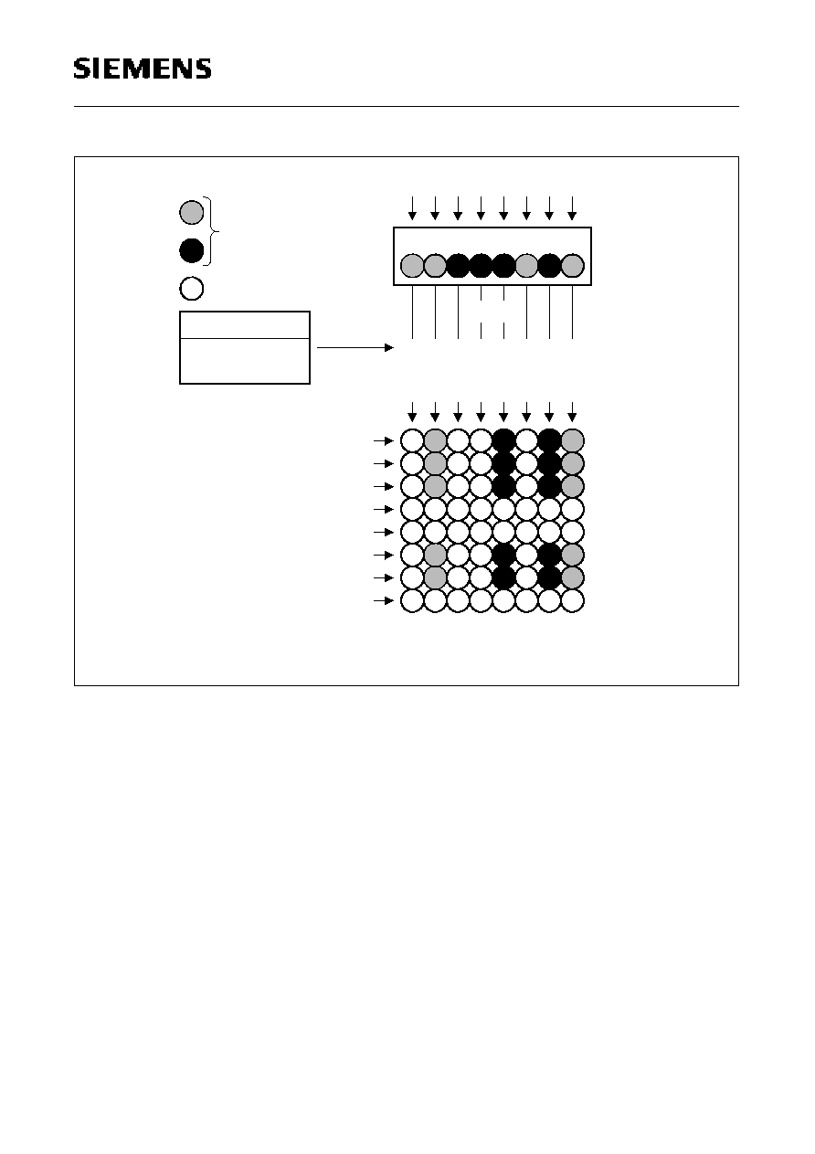
Block Write (BW)
Each Block Write cycle writes a single data value from a Color Register to the block of eight
consecutive column locations addressed by A7 - A3. If Single Color Register Mode is enabled, the
content of Color Register 0 is written. If both Color Registers are enabled, address pin A0 selects
the desired Color Register. Address A0 = 0 selects Color Register 0, address pin A0 = 1 Color
Register 1. The information on the DQs which is registered coincident with the Block Write
command is used to mask specific column/byte combinations within the block.
MR
&
DRAM
Cell
DQ
DQM
SPS03710

HYB 39S16320TQ-6/-7/-8
Semiconductor Group
21
1998-10-01
The table shows the masking of data caused by the registered value on the DQ pins, when data is
transfered from Color Register to the 8 succeeding memory locations addressed in the Write Block
command.
When a "1" is registered, the Color Register data will be written to the corresponding DRAM cells,
subject to the DQM and the WPB masking. The overall Block Write mask consists of a combination
of the DQM signals, the WPB mask register and the column/byte mask information.
Block Write Timing Considerations
A Block Write access requires a time period of
t
BWC
to execute, so in general, the cycle after the
Block Write command should be a NOP. However, Active or Precharge commands to the other
bank are allowed. When following a Block Write with a Precharge command to the same bank,
t
BPL
must be met.
Bit Mask mapping of DQ bits
Address
within Written
Block
Byte within Data Word
Byte 3
Byte 2
Byte 1
Byte 0
0
DQ24
DQ16
DQ8
DQ0
1
DQ25
DQ17
DQ9
DQ1
2
DQ26
DQ18
DQ10
DQ2
3
DQ27
DQ19
DQ11
DQ3
4
DQ28
DQ20
DQ12
DQ4
5
DQ29
DQ21
DQ13
DQ5
6
DQ30
DQ22
DQ14
DQ6
7
DQ31
DQ23
DQ15
DQ7
HYB 39S16320TQ-6/-7/-8
Semiconductor Group
22
1998-10-01
Block Write Illustration
Note: Only single Color Register and Byte 0 of Color Register is used in this example.
Color Register
MDQ7 = 0
MDQ6 = 1
MDQ5 = 0
MDQ4 = 0
MDQ3 = 1
MDQ2 = 0
MDQ1 = 1
MDQ0 = 1
Color Data
i
i + 1
i + 2
i + 3
i + 4
i + 5
i + 6
i + 7
Column Address
DQ0 = 1
DQ1 = 1
DQ2 = 1
DQ3 = 0
DQ4 = 0
DQ5 = 1
DQ6 = 1
DQ7 = 0
Column address mask
from DQ pins
Mask Register
MDQ7 - MDQ0
0 1 0 0 1 0 1 1
Write Data
Mask write, keep original data
Write-per-Bit
Mask Data = Mask Register + DQMi
SPS03711

HYB 39S16320TQ-6/-7/-8
Semiconductor Group
23
1998-10-01
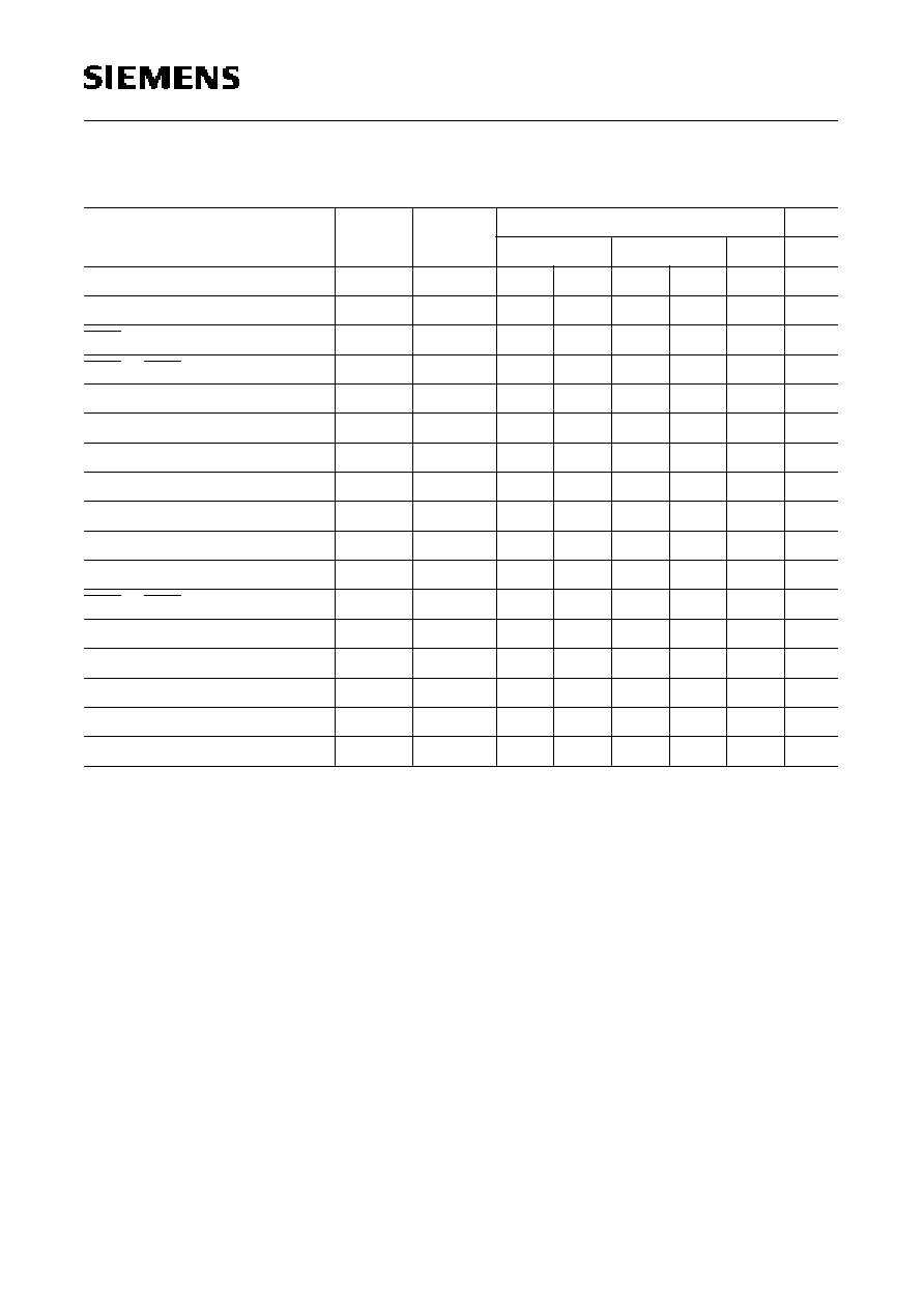
Electrical Characteristics
Absolute Maximum Ratings
Operating temperature range .........................................................................................0 to + 70
�
C
Storage temperature range..................................................................................... � 55 to + 150
�
C
Input/output voltage .......................................................................................... � 0.3 to
V
DD
+ 0.3 V
Power supply voltage
V
DD
/
V
DDQ
............................................................................... � 0.3 to + 4.6 V
Power Dissipation ....................................................................................................................... 1 W
Data out current (short circuit) ................................................................................................ 50 mA
Note: Stresses above those listed under "Absolute Maximum Ratings" may cause permanent
damage of the device. Exposure to absolute maximum rating conditions for extended
periods may affect device reliability.
Notes
1. All voltages are referenced to
V
SS
2.
V
IH
may overshoot to
V
DD
+ 2.0 V for pulse width of < 4 ns with 3.3 V.
V
IL
may undershoot to
�2.0 V for pulse width < 4 ns with 3.3 V. Pulse width measured at 50% points with amplitude
measured peak to DC reference.
Recommended Operation and DC Characteristics
T
A
= 0 to 70
�
C;
V
SS
= 0 V;
V
DD
,
V
DDQ
= 3.3 V
�
0.3 V
Parameter
Symbol
Limit Values
Unit
Notes
min.
max.
Input high voltage
V
IH
2.0
V
DD
+ 0.3
V
1, 2
Input low voltage
V
IL
� 0.3
0.8
V
1, 2
Output high voltage (
I
OUT
= � 2.0 mA)
V
OH
2.4
�
V
Output low voltage (
I
OUT
= 2.0 mA)
V
OL
�
0.4
V
Input leakage current, any input
(0 V <
V
IN
< 3.6 V, all other inputs = 0 V)
I
I(L)
� 5
5
�
A
Output leakage current
(DQ is disabled, 0 V <
V
OUT
<
V
DD
)
I
O(L)
� 5
5
�
A
HYB 39S16320TQ-6/-7/-8
Semiconductor Group
24
1998-10-01
Capacitance
T
A
= 0 to 70
�
C;
V
DD
= 3.3 V
�
0.3 V,
f
= 1 MHz
Parameter
Symbol
max. Values
Unit
Input capacitance (A0 to A9, BA)
C
I1
4
pF
Input capacitance
(RAS, CAS, WE, CS, CLK, CKE, DQM, DSF)
C
I2
4
pF
Output capacitance (DQ)
C
IO
6
pF
Operating Currents
T
A
= 0 to 70
�
C,
V
DD
= 3.3 V
�
0.3 V
(Recommended Operating Conditions unless otherwise noted)
Parameter & Test
Condition
Symb. -6
-7
-8
Unit
Note
max.
Operating current
CAS Latency = 3
CAS Latency = 2
t
RC
t
RC(MIN.)
,
t
CK
t
CK(MIN.)
,
I
O
= 0 mA
I
CC1
200
180
200
180
180
170
mA
2
Precharge standby current
in Power Down Mode
CKE
V
IL(MAX.)
t
CK
=
t
CK(MIN.)
CKE
V
IL(MAX.)
,
t
CK
= infinite
I
CC2P
I
CC2PS
3
2
3
2
3
2
mA
2
Precharge standby current
in Non Power Down Mode
CKE
V
IH(MIN.)
t
CK
t
CK(MIN.)
,
input changed once in 30 ns
CKE
V
IH(MIN.)
,
t
CK
= infinite,
no input change
I
CC2N
I
CC2NS
60
15
60
15
60
15
mA
mA
2
Active standby current in
Power Down Mode
CKE
V
IL(MAX.)
,
t
CK
t
CK(MIN.)
CKE
V
IL(MAX.)
,
t
CK
= infinite
I
CC3P
I
CC3PS
3
3
3
3
3
3
mA
mA
Active standby current in
Non-Power Down Mode
CKE
V
IH(MIN.)
,
t
CK
t
CK(MIN.)
input changed every 30 ns
CKE
V
IH(MIN.)
,
t
CK
= infinite,
no input change
I
CC3N
I
CC3NS
90
30
90
30
90
25
mA
mA
Burst Operating Current
CAS Latency = 3
CAS Latency = 2
Burst Length = full page
t
RC
= infinite
t
CK
t
CK(MIN.)
,
I
O
= 0 mA,
2 banks interleave
I
CC4
200
200
200
200
190
190
mA
mA
2, 3
Auto (CBR) Refresh
Current
CAS Latency = 3
CAS Latency = 2
t
RC
t
RC(MIN.)
I
CC5
170
160
170
160
160
160
mA
2
Self Refresh Current
CKE
0,2 V
2
2
2
mA
Operating Current
(Block Write)
t
CK
t
CK(MIN.)
,
I
O
= 0 mA
t
BWC
=
t
BWC(MIN.)
200 200 190 mA

HYB 39S16320TQ-6/-7/-8
Semiconductor Group
25
1998-10-01
Notes
1. All values are preliminary and subject to future change
2. These parameters depend on the cycle rate and these values are measured by the cycle rate
under the minimum value of
t
CK
and
t
RC
. Input signals are changed one time during t
CK
.
3. These parameters depend on output loading. Specified values are obtained with output open.

HYB 39S16320TQ-6/-7/-8
Semiconductor Group
26
1998-10-01
AC Characteristics
T
A
= 0 to 70
�
C;
V
SS
= 0 V;
V
DD
= 3.3 V
�
0.3 V,
t
T
= 1 ns
Parameter
Symb.
Limit Values
Unit
Note
-6
-7
-8
min.
max.
min.
max.
min.
max.
Clock and Clock Enable
Clock Cycle Time
CAS Latency = 3
CAS Latency = 2
t
CK3
t
CK2
6
8
�
�
7
8
�
�
8
10
�
�
ns
ns
System frequency
CAS Latency = 3
CAS Latency = 2
�
�
�
�
166
125
�
�
143
125
�
�
125
100
MHz
MHz
Clock Access time
(for 30 pF load)
CAS Latency = 3
CAS Latency = 2
t
AC3
t
AC2
�
�
5.5
5.5
�
�
5.5
5.5
�
�
6
6
ns
ns
2
2
Clock High Pulse width
t
CH
2.5
�
3
�
3
�
ns
Clock Low Pulse width
t
CL
2.5
�
2.5
�
3
�
ns
CKE Setup time
t
CKS
2
�
2
�
2.5
�
ns
CKE Hold time
t
CKH
1
�
1
�
1
�
ns
Transition time (rise and fall)
t
T
0.5
10
0.5
10
0.5
10
ns
Common Parameters
Command Setup time
t
CS
2
�
2
�
2.5
�
ns
3
Command Hold time
t
CH
1
�
1
�
1
�
ns
Address Setup time
t
AS
2
�
2
�
2.5
�
ns
3
Address Hold time
t
AH
1
�
1
�
1
�
ns
Active to Read or Write
delay
t
RCD
18
�
21
�
24
�
ns
4
Cycle time
t
RC
66
�
70
�
80
�
ns
4
Active to Precharge
command period
t
RAS
48
100k
49
100k
56
100k
ns
4
Row Precharge time
t
RP
18
�
21
�
24
�
ns
4
Active Bank A to Active
Bank B command period
t
RRD
12
�
14
�
16
�
ns
4
CAS to CAS delay time
(same bank)
t
CCD
1
�
1
�
1
�
CLK
HYB 39S16320TQ-6/-7/-8
Semiconductor Group
27
1998-10-01
Refresh Cycle
Self Refresh Exit time
t
SREX
2
�
2
�
2
�
CLK
5
Total Self Refresh Exit time
�
2 CLKs +
t
RC
�
5
Refresh Period for
Non-Self Refresh
t
REF
�
32
�
32
�
32
ms
6
Read Cycle
Data Out Hold time
t
OH
2.5
�
2.5
�
3
�
ns
Data Out to Low Impedance
time
t
LZ
0
�
0
�
0
�
ns
Data Out to High Impedance
time
t
HZ
3
8
3
8
3
8
ns
7
Write Cycle
Data In Setup time
t
DS
3
�
2
�
2.5
�
ns
Data In Hold time
t
DH
1
�
1
�
1
�
ns
Write recovery time
t
WR
6
�
7
�
8
�
ns
Block Write Cycle
Block Write Cycle Time
t
BWC
12
�
14
�
16
�
ns
Block Write to Precharge
delay
t
BWR
12
�
14
�
16
�
ns
Miscellaneous
Mode Register command to
command
t
RSC
2
�
2
�
2
�
CLK
AC Characteristics (cont'd)
T
A
= 0 to 70
�
C;
V
SS
= 0 V;
V
DD
= 3.3 V
�
0.3 V,
t
T
= 1 ns
Parameter
Symb.
Limit Values
Unit
Note
-6
-7
-8
min.
max.
min.
max.
min.
max.

HYB 39S16320TQ-6/-7/-8
Semiconductor Group
28
1998-10-01
Notes
1. AC timing tests have
V
IL
= 0.4 V and
V
IH
= 2.4 V with the timing referenced to the 1.4 V crossover
point. The transition time is measured between
V
IH
and
V
IL
. All AC measurements assume
t
T
= 1 ns with the AC output load circuit shown.
2. If clock rising time is longer than 1ns, a time (
t
T
/2
-
0.5) ns has to be added to this parameter.
3. If
t
T
is longer than 1 ns, a time (
t
T
-
1) ns has to be added to this parameter.
4. These parameter account for the number of clock cycle and depend on the operating frequency
of the clock, as follows: Number of clock cycle = specified value of timing period (counted in
fractions as a whole number)
5. Self Refresh Exit is a synchronous operation and begins on the second positiv edge after CKE
returns high. Self Refresh Exit is not complete until a time period equal to
t
RC
is satisfied once the
Self Refresh Exit command is registered.
6. Any time that the refresh Period has been exceeded, a minimum of two Auto (CRB) Refresh
commands must be given to "wake-up" the device.
7. Referenced to the time which the output achieves the open circuit condition, not to output voltage
levels.
SPT03404
CLOCK
2.4 V
0.4 V
INPUT
HOLD
t
SETUP
t
t
T
OUTPUT
1.4 V
t
LZ
AC
t
t
AC
OH
t
HZ
t
1.4 V
CL
t
CH
t
50 pF
I/O
Measurement conditions for
t
AC
and
t
OH
HYB 39S16320TQ-6/-7/-8
Semiconductor Group
29
1998-10-01
Clock Frequency and Latency
Parameter
Symbol
Speed Sort
Unit
-6
-7
-8
Clock Frequency
max.
-
166
125
143
125
125
MHz
Clock Cycle time
min.
t
CK
6
8
7
8
8
ns
CAS Latency
min.
t
AA
3
2
3
2
3
CLK
RAS to CAS delay
min.
t
RCD
3
3
3
3
3
CLK
Bank Active Cycle time
min.
t
RAS
8
6
7
6
7
CLK
Bank Active Cycle time
max.
t
RAS
100
100
100
100
100
�
s
Precharge time
min.
t
RP
3
3
3
3
3
CLK
Bank Cycle time
min.
t
RC
11
9
10
9
10
CLK
Last Data In to Precharge
min.
t
WR
1
1
1
1
1
CLK
Last Data In to Active/Refresh
min.
t
WR
+
t
RP
4
4
4
4
4
CLK
Bank to Bank delay time
min.
t
RRD
2
2
2
2
2
CLK
CAS to CAS delay time
min.
t
CCD
1
1
1
1
1
CLK
Write Latency
fixed
t
WL
0
0
0
0
0
CLK
DQM Write Mask Latency
fixed
t
DQW
0
0
0
0
0
CLK
DQM Data Disable Latency
fixed
t
DQZ
2
2
2
2
2
CLK
Clock Suspend Latency
fixed
t
CSL
1
1
1
1
1
CLK
Block Write Cycle time
fixed
t
BWC
2
2
2
2
2
CLK

HYB 39S16320TQ-6/-7/-8
Semiconductor Group
30
1998-10-01
Package Outlines
Plastic Package, P-TQFP-100
Thin Small Outline Package, SMD
(20
�
14 mm
2
, 0.65 mm lead pitch)
Sorts of Packing
Package outlines for tubes, trays etc. are contained in our
Data Book "Package Information".
Dimensions in mm
SMD = Surface Mounted Device

HYB 39S16320TQ-6/-7/-8
Semiconductor Group
31
1998-10-01
Timing Diagrams
1
Bank Activate Command Cycle
2
Burst Read Operation
3
Read Interrupted by a Read
4
Read to Write Interval
4.1
Read to Write Interval
4.2
Minimum Read to Write Interval
4.3
Non-Minimum Read to Write Interval
4.4
Single Bit Write Cycle
5
Burst Write Operation
5.1
Burst Write
5.2
Load Mode Register and Block Write Cycle
5.3
Read and DQM Function
5.4
Write and DQM Function
6
Write and Read Interrupt
6.1
Write Interrupted by a Write
6.2
Write Interrupted by a Read
7
Burst Write and Read with Auto Precharge
7.1
Burst Write with Auto Precharge
7.2
Burst Read with Auto Precharge
8
Burst Termination
8.1
Termination of a Full Page Burst Read Operation
8.2
Termination of a Full Page Burst Write Operation
9
AC Parameters
9.1
AC Parameters for Write Timing
9.2
AC Parameters for Read Timing
10
Mode Register Set
11
Power on Sequence and Auto Refresh (CBR)
12
Clock Suspension (Using CKE)
12.1
Clock Suspension During Burst Read CAS Latency = 2
12.2
Clock Suspension During Burst Read CAS Latency = 3
12.3
Clock Suspension During Burst Write CAS Latency = 2
12.4
Clock Suspension During Burst Write CAS Latency = 3
13
Power Down Mode and Clock Suspend
14
Self Refresh (Entry and Exit)

HYB 39S16320TQ-6/-7/-8
Semiconductor Group
32
1998-10-01
Timing Diagrams (cont'd)
15
Auto Refresh (CBR)
16
Random Column Read (Page within same Bank)
16.1
CAS Latency = 2
16.2
CAS Latency = 3
17
Random Column Write (Page within same Bank)
17.1
CAS Latency = 2
17.2
CAS Latency = 3
18
Random Row Read (Interleaving Banks) with Precharge
18.1
CAS Latency = 2
18.2
CAS Latency = 3
19
Random Row Write (Interleaving Banks) with Precharge
19.1
CAS Latency = 2
19.2
CAS Latency = 3
20
Full Page Read Cycle
20.1
CAS Latency = 2
20.2
CAS Latency = 3
21
Full Page Write Cycle
21.1
CAS Latency = 2
21.2
CAS Latency = 3
22
Precharge Termination of a Burst
22.1
CAS Latency = 2

HYB 39S16320TQ-6/-7/-8
Semiconductor Group
33
1998-10-01
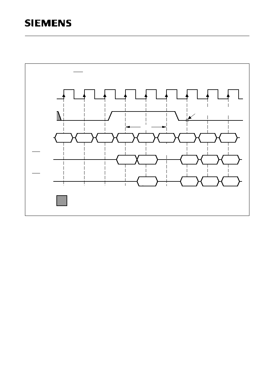
1. Bank Activate Command Cycle
RC
"H" or "L"
t
T0
(CAS latency = 3)
Bank B
Row Addr.
Activate
Bank B
Address
Command
CLK
T
NOP
NOP
RCD
t
T1
Col. Addr.
Bank B
with Auto
Precharge
Write B
T
SPT03784
Bank B
Row Addr.
Activate
Bank B
Row Addr.
Bank A
Activate
Bank A
T
NOP
RRD
t
T
T
HYB 39S16320TQ-6/-7/-8
Semiconductor Group
34
1998-10-01
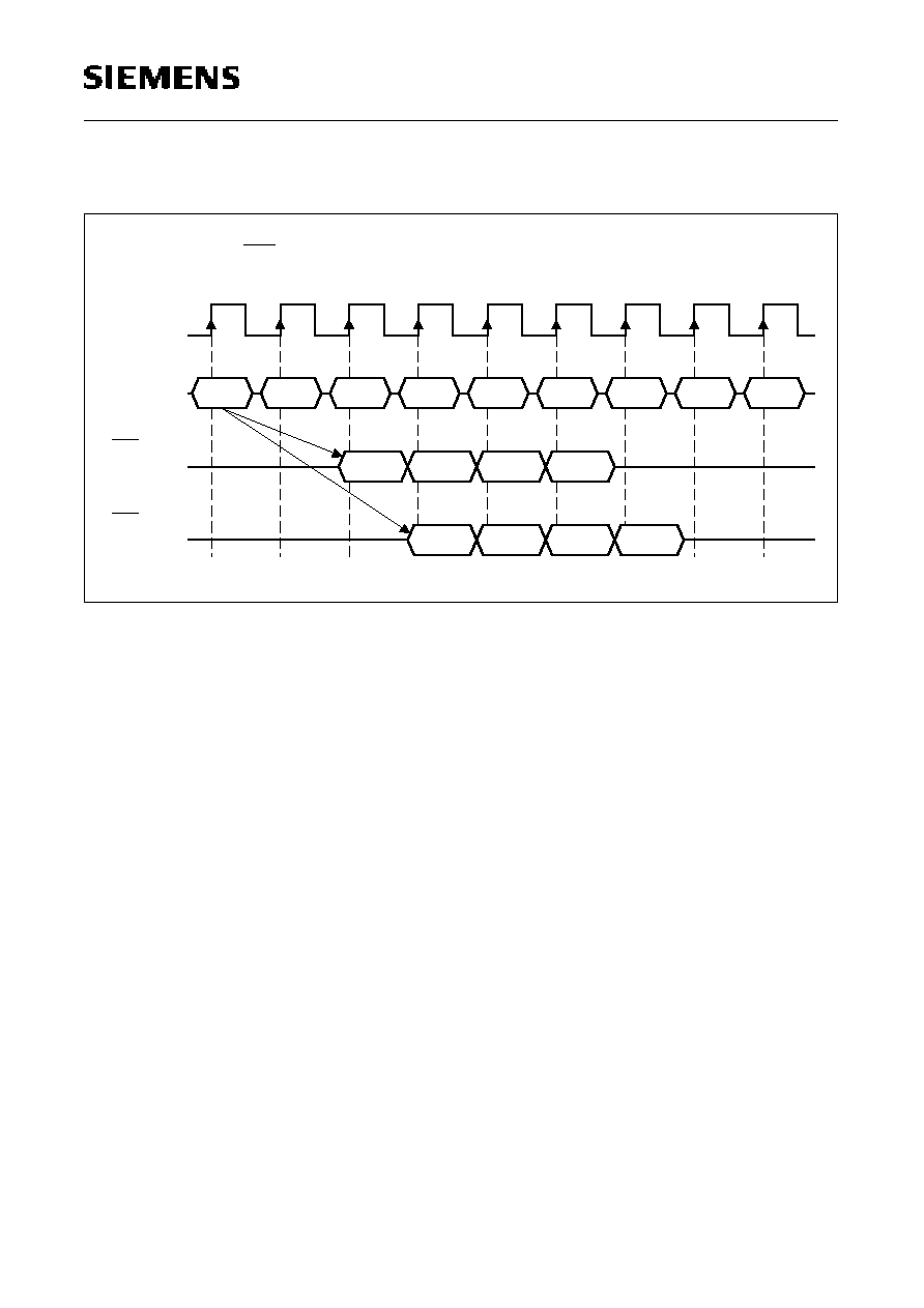
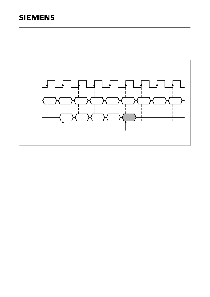
2. Burst Read Operation
SPT03712
CLK
Read A
NOP
T0
T1
T2
T3
T4
T5
T6
T7
T8
Command
NOP
NOP
NOP
NOP
NOP
NOP
NOP
DOUT A3
CK2
latency = 2
t
, DQ's
DOUT A1
DOUT A0
DOUT A2
DOUT A2
CK3
latency = 3
t
, DQ's
DOUT A0 DOUT A1
DOUT A3
(Burst Length = 4, CAS latency = 2, 3)
CAS
CAS

HYB 39S16320TQ-6/-7/-8
Semiconductor Group
35
1998-10-01
3. Read Interrupted by a Read
SPT03713
CLK
Read A
T0
T1
T2
T3
T4
T5
T6
T7
T8
Command
DOUT A0 DOUT B0 DOUT B1 DOUT B2
NOP
NOP
NOP
NOP
NOP
NOP
NOP
latency = 2
, DQ's
CK2
t
CK3
latency = 3
t
, DQ's
(Burst Length = 4, CAS latency = 2, 3)
CAS
CAS
Read B
DOUT B3
DOUT B1
DOUT A0 DOUT B0
DOUT B3
DOUT B2
HYB 39S16320TQ-6/-7/-8
Semiconductor Group
36
1998-10-01
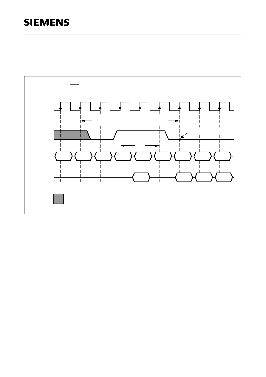
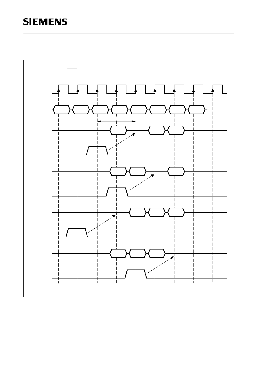
4. Read to Write Interval
4.1. Read to Write Interval
Commands = 4 + 1 = 5 cycles
Minimum delay between the Read and Write
DOUT A0
DQ's
(Burst Length = 4, CAS latency = 3)
DQMx
Command
CLK
NOP
Read A
T0
T1
NOP
NOP
T2
T3
the Write Command
Must be Hi-Z before
DIN B0
DIN B1
SPT03787
DIN B2
DQW
NOP
DQZ
t
NOP
t
T4
T5
Write B
NOP
T6
T7
NOP
T8
"H" or "L"
Write latency
of DQMx

HYB 39S16320TQ-6/-7/-8
Semiconductor Group
37
1998-10-01
4.2. Minimum Read to Write Interval
the Write Command
Must be Hi-Z before
Activate
CAS
CK2
latency = 2
t
, DQ's
(Burst Length = 4, CAS latency = 2)
CLK
DQMx
Command
NOP
T0
T1
Bank A
NOP
DQZ
t
T2
T3
DIN A0
DIN A1
DIN A2
SPT03413
DIN A3
1 Clk Interval
Read A
Write A
T4
T5
NOP
NOP
T6
T7
NOP
T8
"H" or "L"
of DQMx
Write latency
t
DQW
NOP
HYB 39S16320TQ-6/-7/-8
Semiconductor Group
38
1998-10-01
4.3. Non-Minimum Read to Write Interval
CAS
latency = 3
CK3
CAS
CK2
latency = 2
t
t
, DQ's
, DQ's
DOUT A0
(Burst Length = 4, CAS latency = 2, 3)
CLK
DQMx
Command
NOP
Read A
T0
T1
NOP
NOP
T2
T3
the Write Command
Must be Hi-Z before
DOUT A0
DOUT A1
DIN B0
DIN B0
DIN B1
DIN B1
SPT03714
DIN B2
DIN B2
Read A
DQZ
t
NOP
T4
T5
Write B
NOP
T6
T7
NOP
T8
"H" or "L"
of DQMx
Write latency
t
DQW

HYB 39S16320TQ-6/-7/-8
Semiconductor Group
39
1998-10-01
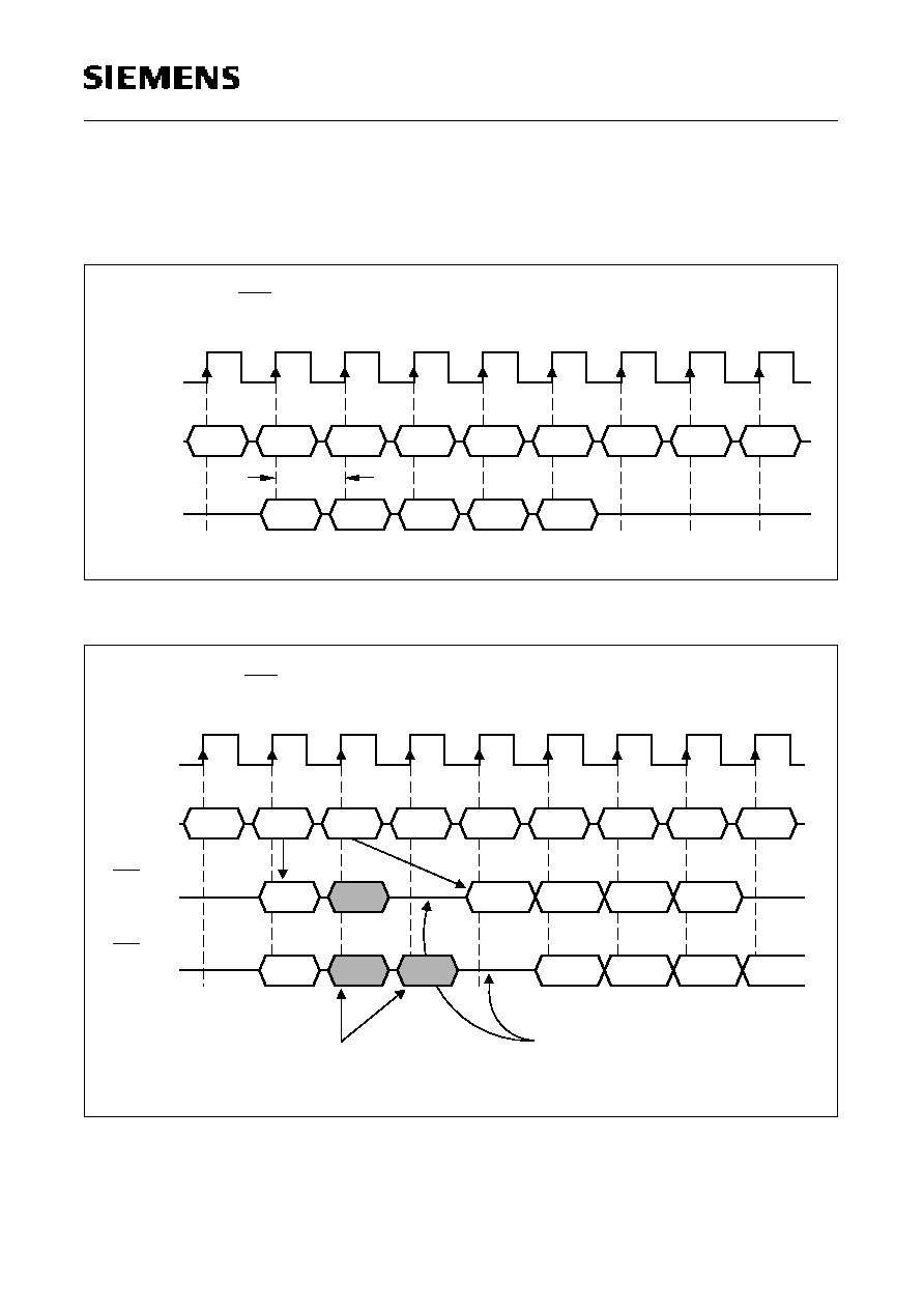
4.4. Single Bit Write Cycle
Burst Write
DQ's
with Write per Bit Enable
"H" or "L"
Bank Activate
(Burst Length = 4, CAS latency = 2, 3)
CLK
DSF
Command
NOP
Bank Activ.
T0
T1
NOP
NOP
T2
T3
DIN B0
DIN B1
DIN B2
DIN B3
SPT03715
Write B
NOP
T4
T5
NOP
NOP
T6
T7
NOP
T8
HYB 39S16320TQ-6/-7/-8
Semiconductor Group
40
1998-10-01
5. Burst Write Operation
5.1. Burst Write
Extra data is ignored after
termination of a Burst.
DIN A3
T4
are registered on the same clock edge.
The first data element and the Write
NOP
(Burst Length = 4, CAS latency = 2, 3)
T0
Command
DQ's
CLK
DIN A1
T2
NOP
DIN A0
Write A
T1
DIN A2
NOP
T3
SPT03790
T6
NOP
NOP
T5
NOP
NOP
T7
NOP
T8
don't care

HYB 39S16320TQ-6/-7/-8
Semiconductor Group
41
1998-10-01
5.2. Load Mode Register and Block Write Cycle
Both Banks must be idle
Load Mode Register
Burst Length set
DQx
A0
Bank Activate
"H" or "L"
(Burst Length = 8, CAS latency = 2, 3)
CLK
Command
DSF
LMR
NOP
RSC
t
T0
T1
ACT
NOP
t
RCD
T2
T3
with Color Reg. 1
SPT03716
with Color Reg. 0
Block Write
Mask
Column
Block Write
Mask
Column
NOP
Block Write
T4
T5
NOP
BWC
t
Block Write
T6
T7
HYB 39S16320TQ-6/-7/-8
Semiconductor Group
42
1998-10-01
5.3. Read and DQM Function
DQ 7...0
(Burst Length = 4, CAS latency = 2)
CLK
Command
NOP
T0
T1
NOP
NOP
T2
T3
SPT03717
NOP
T4
T5
NOP
NOP
T6
T7
T8
NOP
Read
Data 0
Data 3
Data 2
t
DQZ
DQM0
Data 1
Data 3
Data 0
DQ 15...8
DQM1
DQ 23...16
Data 1
Data 3
Data 2
DQM2
Data 1
Data 2
Data 0
DQ 31...24
DQM3

HYB 39S16320TQ-6/-7/-8
Semiconductor Group
43
1998-10-01
5.4. Write and DQM Function
DQ 7...0
(Burst Length = 4, CAS latency = 2)
CLK
Command
NOP
T0
T1
NOP
Write
T2
T3
SPT03718
NOP
T4
T5
NOP
NOP
T6
T7
NOP
Data 0
Data 3
Data 2
DQM0
Data 1
Data 3
Data 0
DQ 15...8
DQM1
DQ 23...16
Data 1
Data 3
Data 2
DQM2
Data 1
Data 2
Data 0
DQ 31...24
DQM3
NOP
HYB 39S16320TQ-6/-7/-8
Semiconductor Group
44
1998-10-01
6. Write and Read Interrupt
6.1. Write Interrupted by a Write
6.2. Write Interrupted by a Read
SPT03791
CLK
T0
T1
T2
T3
T4
T5
T6
T7
T8
Command
NOP
NOP
NOP
NOP
NOP
NOP
DQ's
(Burst Length = 4, CAS latency = 2, 3)
NOP
Write A
DIN A0
DIN B0
DIN B1
DIN B2
DIN B3
Write B
1 Clk Interval
T5
NOP
DOUT B1
DOUT B0
Input data for the Write is ignored.
, DQ's
latency = 3
CK3
CAS
t
don't care
DIN A0
don't care
(Burst Length = 4, CAS latency = 2, 3)
CLK
, DQ's
Command
latency = 2
CK2
CAS
t
NOP
T0
DIN A0
Write A
don't care
Read B
T1
T2
DOUT B0
NOP
NOP
T4
T3
SPT03719
appears on the outputs to avoid data contention.
DOUT B2
Input data must be removed from the DQ's
at least one clock cycle before the Read data
DOUT B1
DOUT B3
NOP
DOUT B3
NOP
DOUT B2
T6
T7
NOP
T8

HYB 39S16320TQ-6/-7/-8
Semiconductor Group
45
1998-10-01
7. Burst Write and Read with Auto Precharge
7.1. Burst Write with Auto Precharge
7.2. Burst Read with Auto Precharge
SPT03720
CLK
Active
NOP
T0
T1
T2
T3
T4
T5
T6
T7
T8
Command
NOP
NOP
NOP
NOP
NOP
NOP
latency = 2
DQ's
latency = 3
DQ's
(Burst Length = 2, CAS latency = 2, 3)
CAS
CAS
Bank A
RP
t
RP
t
Begin Auto Precharge
Bank can be reactivated after
Write A
Auto Precharge
WR
t
DIN A1
DIN A0
WR
t
DIN A1
DIN A0
RP
t
SPT03721
CLK
with AP
NOP
T0
T1
T2
T3
T4
T5
T6
T7
T8
Command
DOUT A0 DOUT A1 DOUT A2 DOUT A3
NOP
NOP
NOP
NOP
NOP
NOP
NOP
latency = 2
, DQ's
CK2
t
DOUT A3
CK3
latency = 3
t
, DQ's
DOUT A1
DOUT A0
DOUT A2
(Burst Length = 4, CAS latency = 2, 3)
CAS
CAS
Read A
RP
t
RP
t
Bank can be reactivated after
Begin Auto Precharge
RP
t

HYB 39S16320TQ-6/-7/-8
Semiconductor Group
46
1998-10-01
8. Burst Termination
8.1. Termination of a Full Page Burst Read Operation
8.2. Termination of a Full Page Burst Write Operation
SPT03722
CLK
NOP
T0
T1
T2
T3
T4
T5
T6
T7
T8
Command
DOUT A0 DOUT A1 DOUT A2 DOUT A3
NOP
NOP
Burst
NOP
NOP
NOP
NOP
latency = 2
, DQ's
CK2
t
DOUT A3
CK3
latency = 3
t
, DQ's
DOUT A1
DOUT A0
DOUT A2
(CAS latency = 2, 3)
CAS
CAS
Read A
The burst ends after a delay equal to the CAS latency.
Terminate
Input data for the Write is masked.
T4
latency = 2, 3
DQ's
NOP
(CAS latency = 2, 3)
T0
Command
CAS
CLK
DIN A1
T2
NOP
DIN A0
Write A
T1
DIN A2
NOP
T3
SPT03419
T6
Burst
Terminate
NOP
T5
NOP
NOP
T7
NOP
T8
don't care

HYB 39S16320TQ-6/-7/-8
Semiconductor Group
47
1998-10-01
9. AC Parameters
9.1. AC Parameters for a Write Timing
Auto Precharge
Bank B
Command
Write with
Activate
Write with
Activate
Bank A
Command
Auto Precharge
Bank A
Command
Command
Bank B
Addr.
A8/AP
DQMx
DQ
BA
Hi-Z
RCD
t
Ax2
Ax1
Ax0
Ax3
RC
t
RAx
RAx
t
AS
t
AH
RBx
RBx
CAx
Activate
Precharge
Activate
Write
Command
Command
Bank A
Bank A
Command
Bank A
Bank A
Command
SPT03723
Bx2
Bx1
Bx0
Bx3
DS
t
t
DH
Ay2
Ay1
Ay0
Ay3
t
WR
RAy
RAy
CBx
RAy
RP
t
RAz
RAz
T8
Precharge
Begin Auto
Bank A
CLK
WE
CAS
RAS
CS
CKE
CK2
t
CS
t
CH
CKS
t
CH
t
t
CL
t
T3
T0
T2
T1
T4
T5
T7
T6
Bank B
Precharge
Begin Auto
t
CKH
T18
Burst Length = 4, CAS Latency = 2
T13
T9
T10
T12
T11
T14 T15
T17
T16
T19 T20
T22
T21
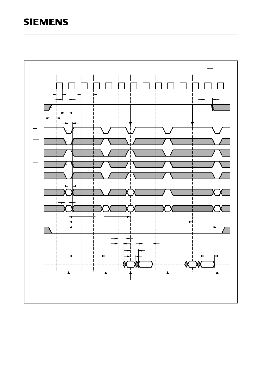
HYB 39S16320TQ-6/-7/-8
Semiconductor Group
48
1998-10-01
9.2. AC Parameters for a Read Timing
y
AC2
Hi-Z
DQ
Activate
Command
Bank A
Read with
Bank A
Command
Auto Precharge
DQMx
Addr.
A8/AP
t
RCD
t
LZ
t
t
AS
RAx
RAx
t
AH
CAx
RRD
t
Command
Bank B
Read with
Auto Precharge
Activate
Bank B
Command
Ax1
Ax0
Bx0
Activate
SPT03724
Command
Bank A
Bx1
t
AC2
OH
t
HZ
t
t
RAS
RC
t
RBx
RBx
RBx
HZ
t
RAy
RAy
T5
t
t
BA
WE
CAS
RAS
t
CS
CKE
CKS
t
CH
t
t
CS
CH
CL
CK2
CLK
T0
T1
T2
T3
T4
Precharge
Bank A
Begin Auto
Precharge
Bank B
Begin Auto
t
CKH
Burst Length = 2, CAS Latency = 2
T6
T7
T8
T10
T9
T11
T13
T12
HYB 39S16320TQ-6/-7/-8
Semiconductor Group
49
1998-10-01
10. Mode Register Set
Set Command
Mode Register
All Banks
Precharge
Command
Any
Command
Address Key
T0
T1
T2
T8
RSC
t
T4
T3
T5
T6
T7
T11
T9
T10
T12 T13
SPT03725
T19
T16
T15
T14
T17 T18
CAS Latency = 2
T20 T21 T22
DSF
A0-A7
A8/AP
CS
WE
CAS
RAS
CKE
CLK

HYB 39S16320TQ-6/-7/-8
Semiconductor Group
50
1998-10-01
11. Power on Sequence and Auto Refresh (CBR)
Inputs must be
200
stable for
�
s
DQMx
A8/AP
DQ
Addr.
BA
RP
Command
All Banks
Precharge
Hi-Z
~ ~
t
1st Auto Refresh
Command
~ ~
~ ~
~ ~
~ ~
~ ~
~ ~
~ ~
SPT03726
Mode Register
Set Command
Address Key
2nd Auto Refresh
Command
~~
t
RC
~~
~~
~~
~ ~
~ ~
~~
~~
Command
Any
Minimum of 8 Refresh Cycles are required
T8
WE
CAS
RAS
CS
CKE
CLK
required
~~
~ ~
~ ~
~ ~
~ ~
~ ~
~ ~
T3
is
~~
~ ~
Level
High
T0
T2
T1
T5
T4
T7
T6
T18
2 Clock min.
~ ~
~ ~
~ ~
~ ~
~ ~
~ ~
~~
T13
~~
~~
T10
T9
T12
T11
T14 T15
T17
T16
T20
T19
T22
T21

HYB 39S16320TQ-6/-7/-8
Semiconductor Group
51
1998-10-01
12. Clock Suspension (Using CKE)
12.1. Clock Suspension During Burst Read CAS Latency = 2
Command
Bank A
DQMx
Addr.
DQ
A8/AP
BA
Read
Command
Bank A
Activate
Hi-Z
Suspend
1 Cycle
Clock
Ax0
CSL
t
Ax1
CAx
RAx
RAx
SPT03727
t
Suspend
3 Cycles
Suspend
2 Cycles
Clock
Ax2
CSL
t
Clock
Ax3
HZ
T7
WE
CAS
RAS
CS
CKE
CLK
CK2
t
T0
T1
T2
T3
T4
T6
T5
T16
T8
T9
T10 T11
T14
T12 T13
T15
Burst Length = 4, CAS Latency = 2
T18
T17
T19 T20 T21 T22
CSL
t
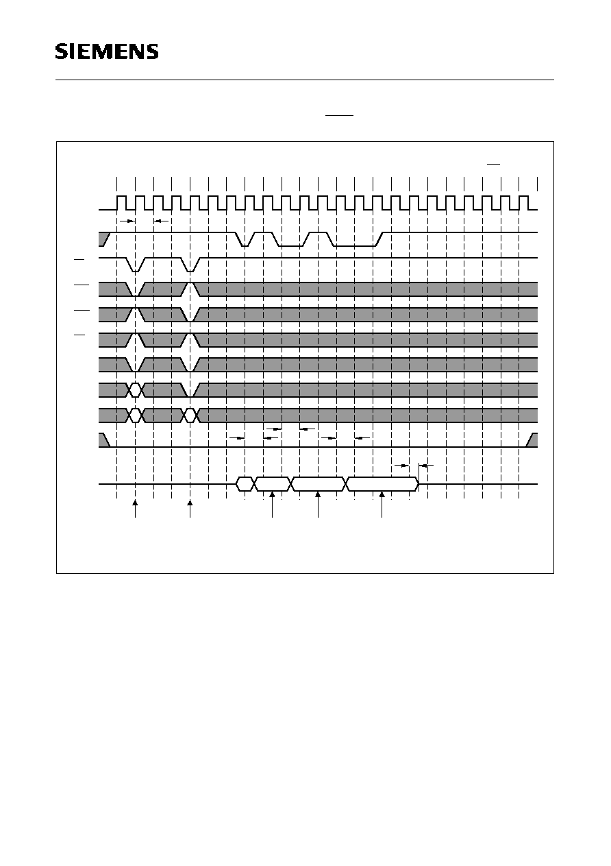
HYB 39S16320TQ-6/-7/-8
Semiconductor Group
52
1998-10-01
12.2. Clock Suspension During Burst Read CAS Latency = 3
CSL
DQMx
Addr.
DQ
A8/AP
BA
Bank A
Activate
Command
Hi-Z
Command
Bank A
Read
Ax0
t
RAx
RAx
CAx
HZ
t
t
Suspend
1 Cycle
Clock
Suspend
2 Cycles
Clock
CSL
Ax1
Ax2
Clock
Suspend
3 Cycles
t
CSL
Ax3
SPT03425
T7
WE
CAS
RAS
CS
CKE
CLK
CK3
t
T0
T1
T2
T3
T4
T6
T5
T16
T8
T9
T10 T11
T14
T12 T13
T15
Burst Length = 4, CAS Latency = 3
T18
T17
T19 T20 T21 T22

HYB 39S16320TQ-6/-7/-8
Semiconductor Group
53
1998-10-01
12.3. Clock Suspension During Burst Write CAS Latency = 2
Bank A
DQMx
Addr.
DQ
A8/AP
BA
DAx0
Command
Write
Activate
Command
Bank A
Hi-Z
Clock
Clock
1 Cycle
Suspend
Suspend
2 Cycles
DAx1
CAx
RAx
RAx
DAx3
Clock
Suspend
3 Cycles
DAx2
SPT03728
T7
WE
CAS
RAS
CS
CKE
CLK
CK2
t
T0
T1
T2
T3
T4
T6
T5
T16
T8
T9
T10 T11
T14
T12 T13
T15
Burst Length = 4, CAS Latency = 2
T18
T17
T19 T20 T21 T22
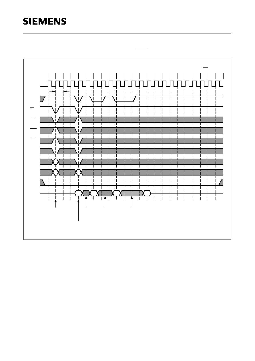
HYB 39S16320TQ-6/-7/-8
Semiconductor Group
54
1998-10-01
12.4. Clock Suspension During Burst Write CAS Latency = 3
Clock
Suspend
2 Cycles
Bank A
DQMx
Addr.
DQ
A8/AP
BA
Activate
Command
Bank A
Hi-Z
Clock
1 Cycle
Suspend
Command
Write
DAx0
DAx1
RAx
RAx
CAx
Clock
Suspend
3 Cycles
DAx2
DAx3
SPT03427
T7
WE
CAS
RAS
CS
CKE
CLK
CK3
t
T0
T1
T2
T3
T4
T6
T5
T16
T8
T9
T10 T11
T14
T12 T13
T15
Burst Length = 4, CAS Latency = 3
T18
T17
T19 T20 T21 T22
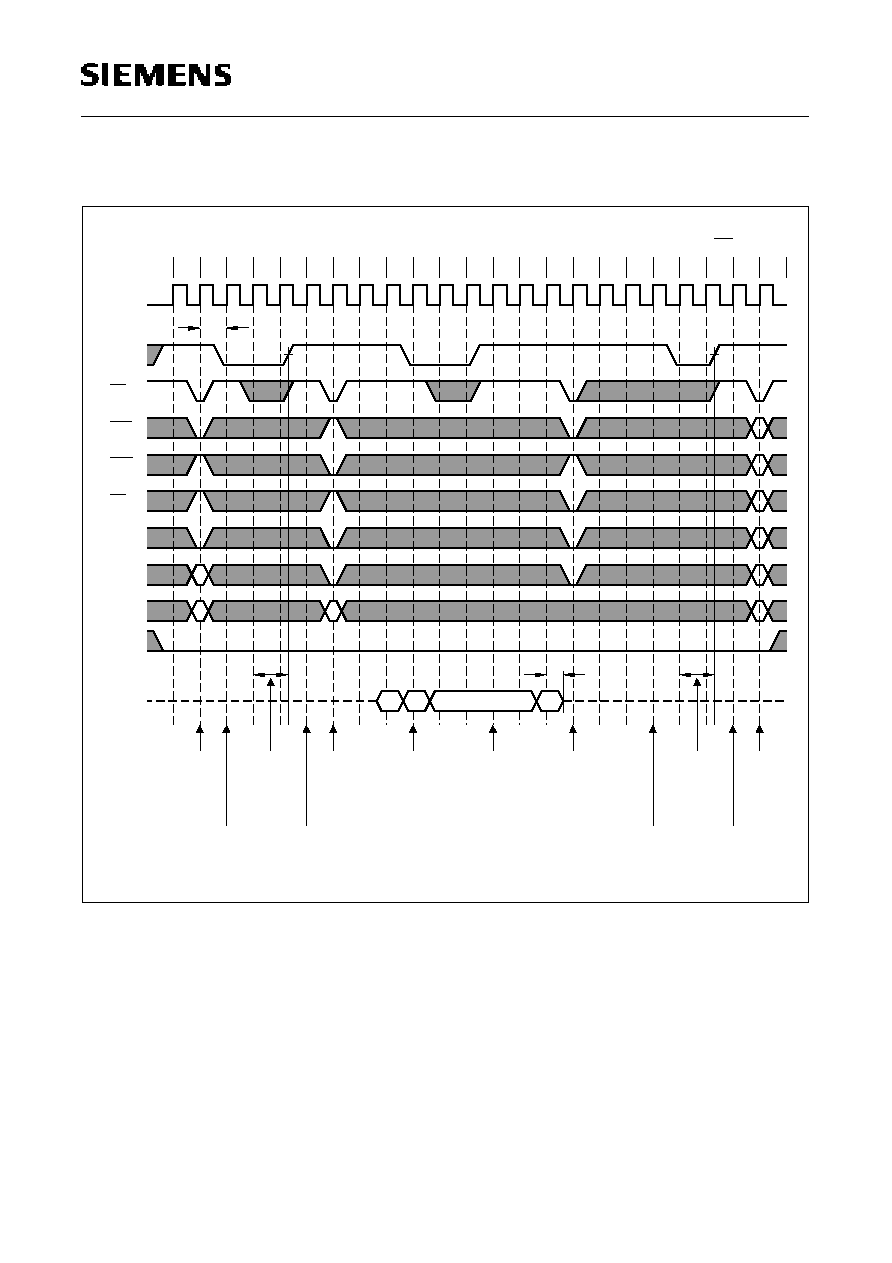
HYB 39S16320TQ-6/-7/-8
Semiconductor Group
55
1998-10-01
13. Power Down Mode and Clock Suspend
BA
Clock Suspend
Clock Suspend
Mode Entry
Mode Exit
Addr.
DQMx
DQ
A8/AP
Standby
Active
Activate
Bank A
Command
Hi-Z
Read
Command
Bank A
RAx
RAx
CAx
Power Down
Power Down
Mode Exit
Mode Entry
SPT03938
End
Clock Mask
Clock Mask
Start
Ax0 Ax1
Ax2
Precharge
Command
Bank A
Ax3
t
HZ
Precharge
Standby
Any
Command
T7
CAS
WE
RAS
CS
CKE
CLK
CK2
t
T0
T1
T2
T3
T4
T6
T5
T16
T8
T9
T10 T11
T14
T12 T13
T15
Burst Length = 4, CAS Latency = 2
T18
T17
T19 T20 T21 T22
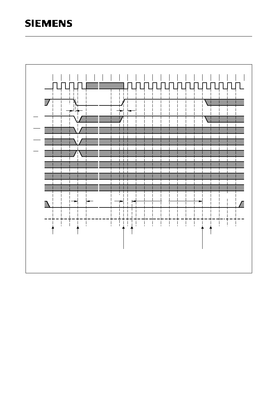
HYB 39S16320TQ-6/-7/-8
Semiconductor Group
56
1998-10-01
14. Self Refresh (Entry and Exit)
BA
t
Self Refresh Exit
Command issued
Addr.
DQMx
DQ
A8/AP
Entry
Self Refresh
must be idle
All Banks
Hi-Z
~ ~
t
SB
~ ~
~ ~
~ ~
~ ~
~ ~
~ ~
SPT03429
Exit Command
Begin Self Refresh
SREX
t
RC
Self Refresh
Command
Exit
Any
T7
CS
CAS
WE
RAS
CKE
CLK
~ ~
~ ~
~ ~
~ ~
~ ~
~ ~
~ ~
~ ~
t
CKH
T0
T1
T2
~ ~
~ ~
T3
T4
~~
~~
T6
T5
T16
CKS
t
T8
T9
T10 T11
T14
T12 T13
T15
T18
T17
T19 T20 T21 T22
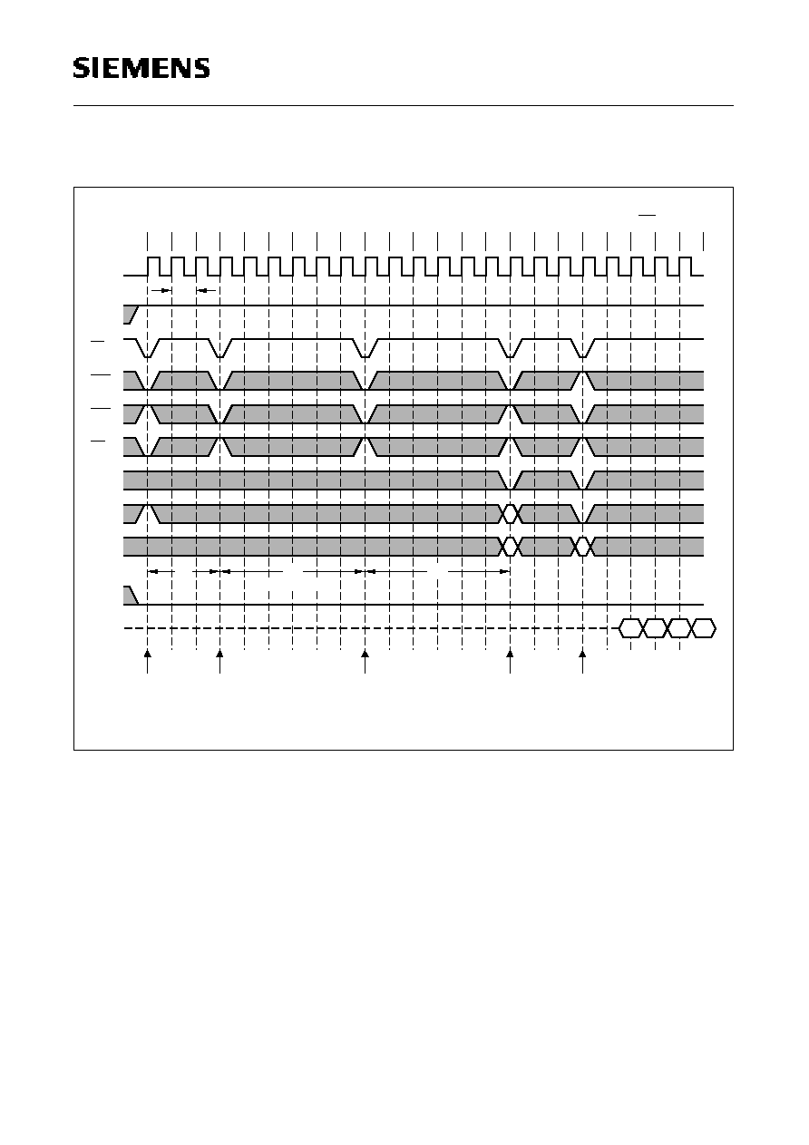
HYB 39S16320TQ-6/-7/-8
Semiconductor Group
57
1998-10-01
15. Auto Refresh (CBR)
(Minimum Interval)
Addr.
DQMx
DQ
A8/AP
BA
Auto Refresh
Command
All Banks
Precharge
Command
Hi-Z
t
RP
t
RC
SPT03729
Command
Command
Auto Refresh
Command
Bank A
Activate
RC
t
RAx
RAx
Ax2
Bank A
Read
Ax0 Ax1
Ax3
CAx
T7
WE
CAS
RAS
CS
CKE
CLK
CK2
t
T0
T1
T2
T3
T4
T6
T5
T16
T8
T9
T10 T11
T14
T12 T13
T15
Burst Length = 4, CAS Latency = 2
T18
T17
T19 T20 T21 T22

HYB 39S16320TQ-6/-7/-8
Semiconductor Group
58
1998-10-01
16. Random Column Read (Page within same Bank)
16.1. CAS Latency = 2
Ay3
CAw
Addr.
BA
DQ
DQMx
A8/AP
Hi-Z
Bank A
Activate
Command
Read
Command
Bank A
RAw
RAw
Bank A
Command
Aw1
Aw0
Read
Bank A
Command
Aw2 Aw3
CAx
Read
Ax1
Ax0
Ay0
Precharge
Command
Bank A
Ay1 Ay2
CAy
CS
WE
CAS
RAS
CKE
CLK
T0
CK2
t
T1
T2
T8
T4
T3
T5
T6
T7
T11
T9
T10
T12 T13
Bank A
Read
Command
Activate
Command
Bank A
Az0
RAz
RAz
CAz
SPT03730
Az1
Burst Length = 4, CAS Latency = 2
T19
T16
T15
T14
T17 T18
T20 T21 T22

HYB 39S16320TQ-6/-7/-8
Semiconductor Group
59
1998-10-01
16.2. CAS Latency = 3
Ay1
Addr.
BA
DQ
DQMx
A8/AP
Activate
Command
Hi-Z
Bank A
RAw
RAw
Command
Read
Command
Bank A
Read
Bank A
Aw0 Aw1
CAw
CAx
Read
Bank A
Command
Aw3
Aw2
Ax0 Ax1 Ay0
CAy
CS
WE
CAS
RAS
CKE
CLK
T0
CK3
t
T1
T2
T8
T4
T3
T5
T6
T7
T11
T9
T10
T12 T13
Precharge
Command
Bank A
Ay2 Ay3
Activate
Command
Bank A
RAz
RAz
SPT03432
Read
Bank A
Command
CAz
Burst Length = 4, CAS Latency = 3
T19
T16
T15
T14
T17 T18
T20 T21 T22

HYB 39S16320TQ-6/-7/-8
Semiconductor Group
60
1998-10-01
17. Random Column Write (Page within same Bank)
17.1. CAS Latency = 2
CBx
DBx0
Bank B
Command
Write
Addr.
DQMx
DQ
A8/AP
BA
Command
Bank B
Activate
Bank B
Command
Hi-Z
Write
DBw2
DBw1
DBw0
DBw3
RBz
RBz
CBz
Command
Bank B
Activate
DBy2
Write
Command
Bank B
DBy0
DBx1
DBy1
Precharge
Command
Bank B
DBy3
CBy
RBz
RBz
DBz3
Write
Command
Bank B
DBz0 DBz1 DBz2
SPT03731
CBz
CAS
RAS
CKE
CLK
WE
CS
T2
CK2
t
T0
T1
T3
T4
T5
T6
T15
T7
T8
T9
T10
T13
T12
T11
T14
Burst Length = 4, CAS Latency = 2
T19
T17
T16
T18
T20 T21 T22
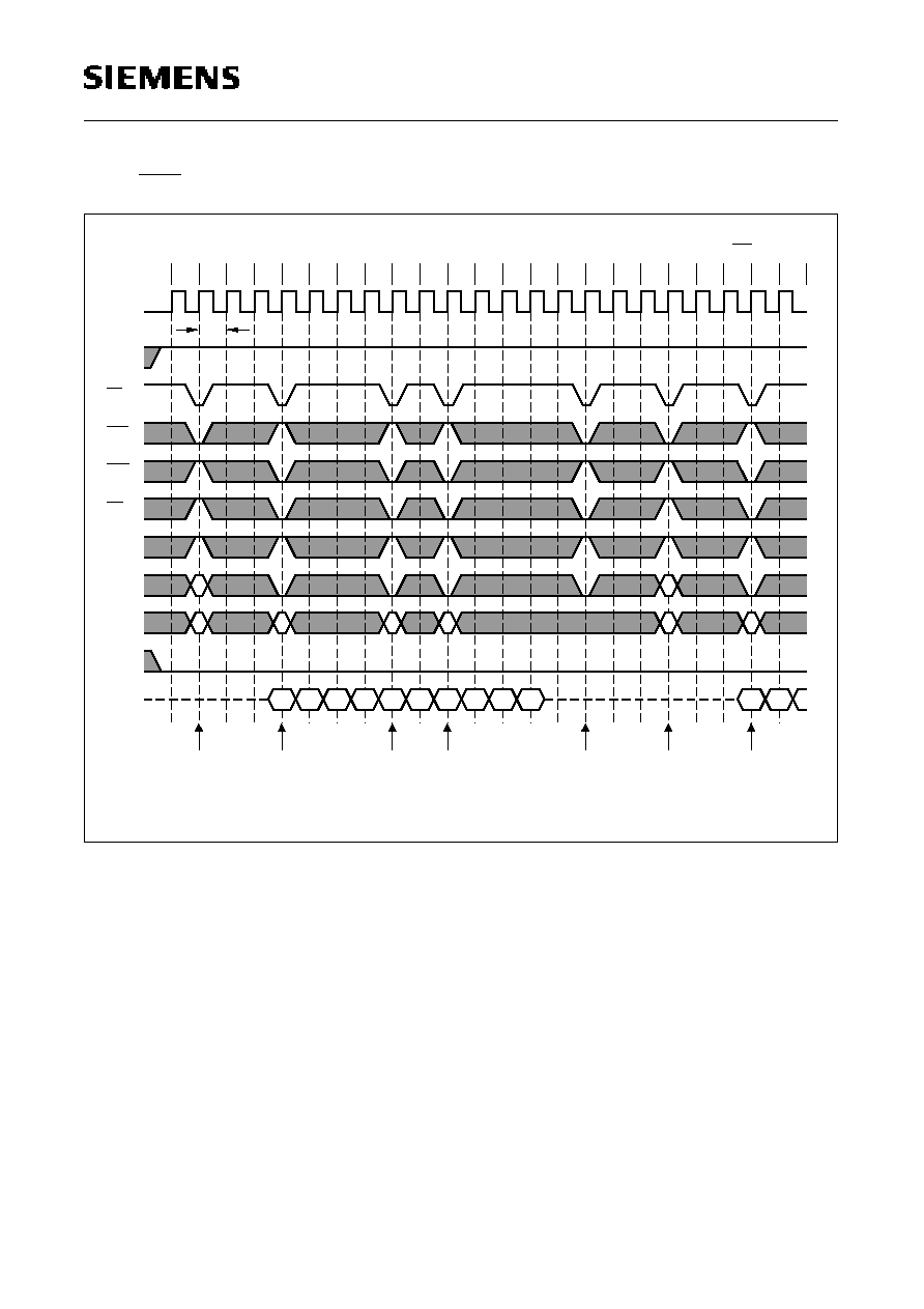
HYB 39S16320TQ-6/-7/-8
Semiconductor Group
61
1998-10-01
17.2. CAS Latency = 3
DBw3
Addr.
DQMx
DQ
A8/AP
BA
Activate
Bank B
Command
Hi-Z
Write
Bank B
Command
DBw1
DBw0
DBw2
RBz
RBz
CBz
Command
Precharge
Write
Write
Bank B
Command
Command
Bank B
DBx1
DBx0
DBy0 DBy1
Bank B
DBy2 DBy3
CBx
CBy
Activate
Command
Bank B
Write
SPT03434
Command
Bank B
DBz1
DBz0
RBz
RBz
CBz
CAS
RAS
CKE
CLK
WE
CS
T2
CK3
t
T0
T1
T3
T4
T5
T6
T15
T11
T7
T8
T10
T9
T13
T12
T14
Burst Length = 4, CAS Latency = 3
T17
T16
T18 T19 T20 T21 T22
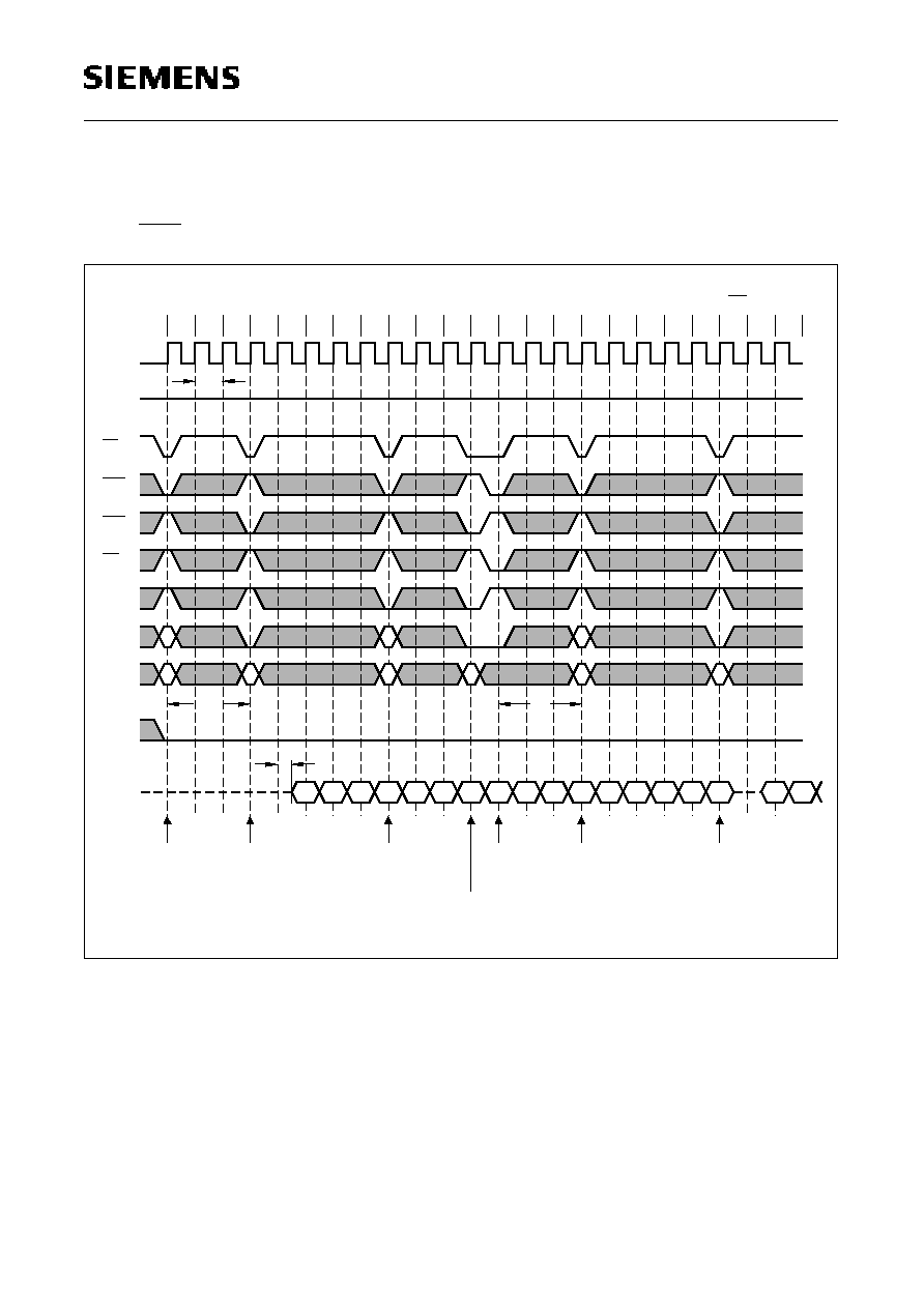
HYB 39S16320TQ-6/-7/-8
Semiconductor Group
62
1998-10-01
18. Random Row Read (Interleaving Banks) with Precharge
18.1. CAS Latency = 2
Ax2
t
BA
Addr.
DQ
DQMx
A8/AP
Bank B
Activate
Command
Hi-Z
Command
Read
Bank B
RBx
RBx
RCD
t
CBx
Read
Activate
Bank A
Command
Command
Bank B
Command
Bx2
Bx0
AC2
Bx1
Bank A
Activate
Bx3 Bx4
RAx
RAx
Command
Precharge
Bank B
Bx6
Bx5
Bx7 Ax0 Ax1
CAx
RP
t
RBy
RBy
CS
WE
CAS
RAS
CKE
CLK
T0
High
t
CK2
T1
T2
T8
T4
T3
T5
T6
T7
T11
T9
T10
T12 T13
SPT03732
Bank B
Command
Ax5
Ax3 Ax4
Read
Ax6 Ax7
CBy
By1
By0
Burst Length = 8, CAS Latency = 2
T19
T16
T15
T14
T17 T18
T20 T21 T22

HYB 39S16320TQ-6/-7/-8
Semiconductor Group
63
1998-10-01
18.2. CAS Latency = 3
Activate
Command
Bank A
Addr.
DQMx
DQ
A8/AP
BA
Read
Bank B
Command
Command
Bank B
Activate
Hi-Z
Bx1
Bx0
CBx
RBx
RCD
t
RBx
t
AC3
Activate
Command
Bank B
Bx6
Bank A
Command
Read
Bx4
Bx3
Bx2
Bx5
Bank B
Precharge
Command
Ax0
Bx7
Ax2
Ax1
RAx
CAx
RAx
RP
t
RBy
RBy
Precharge
Bank A
Command
Ax7
Read
Bank B
Command
Ax5
Ax4
Ax3
Ax6
SPT03436
By0
CBy
T7
WE
CAS
RAS
CS
CKE
CLK
High
CK3
t
T0
T1
T2
T3
T4
T6
T5
T16
T8
T9
T10 T11
T14
T12 T13
T15
Burst Length = 8, CAS Latency = 3
T18
T17
T19 T20 T21 T22
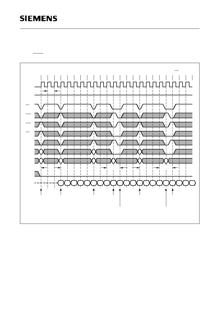
HYB 39S16320TQ-6/-7/-8
Semiconductor Group
64
1998-10-01
19. Random Row Write (Interleaving Banks) with Precharge
19.1. CAS Latency = 2
DBx4
DAx1
BA
A8/AP
Addr.
DQ
DQMx
Activate
Command
Bank A
Hi-Z
Write
Command
Bank A
DAx0
RAx
RAx
RCD
t
CAx
Command
Command
Bank B
Bank A
Command
DAx4
DAx2 DAx3
Bank B
Activate
DAx5 DAx6
RBx
RBx
Command
Precharge
Bank A
Write
DBx0
DAx7
DBx1
Activate
DBx2 DBx3
WR
CBx
t
RP
t
RAy
RAy
CLK
CKE
CS
RAS
CAS
WE
T0
High
CK2
t
T1
T2
T8
T4
T3
T5
T6
T7
T11
T9
T10
T12 T13
Command
Bank A
SPT03733
Command
Precharge
Bank B
DBx7
DBx5 DBx6
Write
DAy0 DAy1
CAy
WR
t
DAy4
DAy3
DAy2
T19
Burst Length = 8, CAS Latency = 2
T16
T15
T14
T17 T18
T20 T21 T22

HYB 39S16320TQ-6/-7/-8
Semiconductor Group
65
1998-10-01
19.2. CAS Latency = 3
DAx4
Addr.
DQMx
DQ
A8/AP
BA
Command
Bank A
Bank A
Activate
Command
Hi-Z
Write
DAx0 DAx1
DAx3
DAx2
RAx
RCD
t
RAx
CAx
DBx4
DBx0
Write
Command
Bank B
Bank B
Activate
Command
DAx6
DAx5
DAx7
Precharge
Command
Bank A
DBx2
DBx1
DBx3
CBx
RBx
RBx
WR
t
RP
t
Command
Bank A
Activate
Command
Bank A
Write
DBx5 DBx6
DAy0
DBx7
Precharge
Bank B
Command
SPT03438
DAy1 DAy2 DAy3
WR
RAy
t
CAy
RAy
CAS
RAS
CKE
CLK
WE
CS
T2
High
CK3
t
T0
T1
T4
T3
T5
T6
T15
T7
T8
T9
T10 T11 T12 T13 T14
Burst Length = 8, CAS Latency = 3
T19
T17
T16
T18
T21
T20
T22

HYB 39S16320TQ-6/-7/-8
Semiconductor Group
66
1998-10-01
20. Full Page Read Cycle
20.1. CAS Latency = 2
BA
-
page address back to zero
from the highest order
The burst counter wraps
during this time interval.
Addr.
DQMx
DQ
A8/AP
~~
Hi-Z
Command
Command
Bank A
Read
Bank A
Activate
Bank B
Bank B
Command
Command
Ax
Activate
Activate
Ax
+1 Ax
~~
+ 2 Ax
RAx
RAx
CAx
~ ~
~ ~
RBx
RBx
~ ~
~ ~
~ ~
~ ~
SPT03734
bursting beginning with the starting address.
Burst Stop
Command
the burst counter increments and continues
terminate when the burst length is satisfied;
Full Page burst operation does not
Bank B
Command
Ax
Read
-
2
Ax 1
1
Ax +
Bx
Bx +1 Bx +2
+
Bx 3
+
Bx 4
CBx
Bank B
Command
Activate
Command
Bank B
Precharge
Bx
5
Bx+
6
+
RBy
t
RP
RBy
CAS
RAS
CKE
CLK
CS
WE
~ ~
~ ~
~ ~
~ ~
~ ~
~ ~
~ ~
High
CK2
t
T0
T1
T2
~ ~
~ ~
T3
T4
~ ~
~ ~
T5
T6
T15
T11
T7
T8
T10
T9
T13
T12
T14
Burst Length = Full Page, CAS Latency = 2
T16 T17 T18 T19 T20 T21 T22

HYB 39S16320TQ-6/-7/-8
Semiconductor Group
67
1998-10-01
20.2. CAS Latency = 3
T14
Bx
Full Page burst operation does not
terminate when the burst length is satisfied;
bursting beginning with the starting address.
the burst counter increments and continues
BA
Command
Bank A
A8/AP
DQMx
DQ
Addr.
Command
Activate
Bank A
Hi-Z
Read
RAx
RAx
CAx
page address back to zero
during this time interval.
The burst counter wraps
from the highest order
Activate
Activate
Bank B
Bank B
Command
Command
Ax
Ax 1
+
2
Ax +
Ax
~~
~~
-
RBx
RBx
~~
~~
~~
~~
~~
~~
Ax
Read
Bank B
Command
Ax
2
1
-
Ax
1
+
Bx
Bx 1
+
CBx
T3
CLK
CKE
CS
RAS
WE
CAS
T0
High
CK3
t
T1
T2
~~
~~
~~
~~
~~
~~
~~
T4
T5
~ ~~
~
~~
T7
T6
T8
~~
T10
T9
T11
T13
T12
SPT03440
Bank B
Command
Activate
Bank B
Precharge
Command
Burst Stop
Command
+
+2 Bx
Bx
3
4
+
5
+
Bx
RBy
t
RP
RBy
T20
Burst Length = Full Page, CAS Latency = 3
T17
T15 T16
T18 T19
T21 T22

HYB 39S16320TQ-6/-7/-8
Semiconductor Group
68
1998-10-01
21. Full Page Write Cycle
21.1. CAS Latency = 2
T14
DBx
~ ~
Command
Activate
Command
Activate
Addr.
A8/AP
DQMx
DQ
Command
Bank A
Activate
Write
Command
Bank A
Hi-Z
RAx
RAx
DAx
DAx 1
+
CAx
page address back to zero
the burst counter increments and continues
bursting beginning with the starting address.
during this time interval.
CBx
DBx
Write
Bank B
terminate when the burst length is satisfied;
Command
from the highest order
The burst counter wraps
Bank B
Bank B
1
DAx
+
DAx 2
~~
~~
+3 DAx-
~~
RBx
RBx
~ ~~
~
~~
DAx
DAx+1
Full Page burst operation does not
Data is
ignored.
DBx
DBx+1
+
DBx 2
4
3
+
DBx+
DBx 5
+
T3
CLK
CKE
CS
CAS
RAS
BA
WE
T0
High
CK2
t
T1
T2
~ ~~
~
~~
~
~
~~
~
~
~~
~
~
~~
~~
T4
~~
T5
~~
T7
T6
T8
T10
T9
T11
T13
T12
SPT03735
Precharge
Command
Bank B
Burst Stop
Command
Command
Bank B
Activate
+6
RBy
RBy
T20
T17
T15 T16
T18 T19
T21 T22
Burst Length = Full Page, CAS Latency = 2

HYB 39S16320TQ-6/-7/-8
Semiconductor Group
69
1998-10-01
21.2. CAS Latency = 3
T14
Full Page burst operation does not
DBx
bursting beginning with the starting address.
the burst counter increments and continues
terminate when the burst length is satisfied;
Command
Bank A
A8/AP
DQ
Addr.
DQMx
Command
Activate
Bank A
Write
Hi-Z
RAx
RAx
DAx
CAx
from the highest order
during this time interval.
page address back to zero
+
The burst counter wraps
Command
Bank B
Activate
Bank B
Command
Activate
DAx
+
DAx 1
+ 2 DAx+
RBx
RBx
DAx
3
~~
~~
1
-
~ ~
DAx DAx
~~
~ ~
~~
~ ~
Bank B
Command
Write
ignored.
Data is
DBx
DBx
1
+
DBx 1
CBx
3
+ 2
+
DBx
DBx+ 4
T3
CS
WE
BA
CAS
RAS
CKE
CLK
T0
High
CK3
t
T1
T2
~~
~ ~
~~
~ ~
~~
~ ~
~~
~ ~
T4
T5
~ ~
~ ~
T7
~~~
~
T6
T8
T10
T9
T11
T13
T12
SPT03442
Command
Bank B
Activate
Precharge
Command
Bank B
Command
Command
Burst Stop
Burst Stop
+ 5
RBy
RBy
Burst Length = Full Page, CAS Latency = 3
T20
T17
T15 T16
T18 T19
T21 T22

HYB 39S16320TQ-6/-7/-8
Semiconductor Group
70
1998-10-01
22. Precharge Termination of a Burst
22.1. CAS Latency = 2
BA
RP
of a Write Burst.
Write Data is masked.
DQMx
A8/AP
DQ
Addr.
Command
Precharge Termination
Bank A
Activate
Command
Bank A
Write
Hi-Z
DAx0
Bank A
Precharge
Command
DAx3
DAx2
DAx1
CAx
RAx
RAx
t
of a Read Burst.
SPT03736
Command
Bank A
Activate
Command
Bank A
Activate
Command
Bank A
Read
Command
Precharge
Bank A
Ay1
Ay0
Ay2
CAy
RAy
RAy
t
RP
Precharge Termination
Bank A
Command
Read
CAz
RAz
RAz
T8
CAS
WE
RAS
CS
CKE
CLK
T3
t
High
CK2
T0
T2
T1
T5
T4
T6
T7
T18
Burst Length = 8 or Full Page, CAS Latency = 2
T13
T9
T10
T12
T11
T15
T14
T16 T17
T19 T20
T22
T21