Semiconductor Group
1
3.3V 2M x 64/72-Bit 1 BANK SDRAM Module
3.3V 4M x 64/72-Bit 2 BANK SDRAM Module
168 pin unbuffered DIMM Modules
HYS64/72V2200GU-8/-10
HYS64/72V4220GU-8/-10
∑
168 Pin PC100 and PC66 compatible unbuffered 8 Byte Dual-In-Line SDRAM Modules
for PC main memory applications
∑
1 bank 2M x 64, 2M x 72 and 2 bank 4M x 64, 4M x 72 organisation
∑
Optimized for byte-write non-parity or ECC applications
∑
JEDEC standard Synchronous DRAMs (SDRAM)
∑
Fully PC board layout compatible to INTEL's Rev. 1.0 module specification
∑
SDRAM Performance:
∑
Programmed Latencies :
∑
Single +3.3V(
±
0.3V ) power supply
∑
Programmable CAS Latency, Burst Length and Wrap Sequence
(Sequential & Interleave)
∑
Auto Refresh (CBR) and Self Refresh
∑
Decoupling capacitors mounted on substrate
∑
All inputs, outputs are LVTTL compatible
∑
Serial Presence Detect with E
2
PROM
∑
Utilizes 2M x 8 SDRAMs in TSOPII-44 packages
∑
4096 refresh cycles every 64 ms
∑
133,35 mm x 31.75 mm x 4,00 mm card size with gold contact pads
-8
-8-3
-10
Units
f
CK
Clock frequency (max.)
100
100
66
MHz
t
AC
Clock access time
6
6
8
ns
Product Speed
CL
tRCD
tRP
-8
PC100
2
2
2
-8-3
PC100
3
2
3
-10
PC66
2
2
2
1
6.98
HYS64(72)V2200/4220GU-8/-10
SDRAM-Modules
Semiconductor Group
2
The HYS64(72)2200 and HYS64(72)4220 are industry standard 168-pin 8-byte Dual in-line Memory Modules
(DIMMs) which are organised as 2M x 64, 2M x 72 in 1 bank and 4M x 64 and 4M x 72 in two banks high speed
memory arrays designed with Synchronous DRAMs (SDRAMs) for non-parity and ECC applications. The DIMMs
use -8 speed sort 2M x 8 SDRAM devices in TSOP44 packages to meet the PC100 requirement. Modules which
use -10 parts are suitable for PC66 applications only. Decoupling capacitors are mounted on the PC board. The
PC board design is according to INTEL's PC SDRAM Rev.1.0 module specification.
The DIMMs have a serial presence detect, implemented with a serial E
2
PROM using the two pin I
2
C protocol. The
first 128 bytes are utilized by the DIMM manufacturer and the second 128 bytes are available to the end user.
All SIEMENS 168-pin DIMMs provide a high performance, flexible 8-byte interface in a 133,35 mm long footprint,
with 1,25" ( 31,75 mm) height
Ordering Information
Pin Names
Address Format:
Type
Ordering Code
Package
Descriptions
Module
Height
HYS 64V2200GU-8
PC100-222-620
L-DIM-168-29
100 Mhz 2M x 64 1 bank SDRAM module
1,25"
HYS 72V2200GU-8
PC100-222-620
L-DIM-168-29
100 MHz 2M x 72 1 bank SDRAM module
1,25"
HYS 64V4220GU-8
PC100-222-620
L-DIM-168-29
100 Mhz 4M x 64 2 bank SDRAM module
1,25"
HYS 72V4220GU-8
PC100-222-620
L-DIM-168-29
100 Mhz 4M x 72 2 bank SDRAM module
1,25"
HYS 64V2200GU-8-3
PC100-323-620
L-DIM-168-29
100 Mhz 2M x 64 1 bank SDRAM module
1,25"
HYS 72V2200GU-8-3
PC100-323-620
L-DIM-168-29
100 MHz 2M x 72 1 bank SDRAM module
1,25"
HYS 64V4220GU-8-3
PC100-323-620
L-DIM-168-29
100 Mhz 4M x 64 2 bank SDRAM module
1,25"
HYS 72V4220GU-8-3
PC100-323-620
L-DIM-168-29
100 Mhz 4M x 72 2 bank SDRAM module
1,25"
HYS 64V2200GU-10
PC66-222-920
L-DIM-168-29
66 Mhz 2M x 64 1 bank SDRAM module
1,25"
HYS 72V2200GU-10
PC66-222-920
L-DIM-168-29
66 MHz 2M x 72 1 bank SDRAM module
1,25"
HYS 64V4220GU-10
PC66-222-920
L-DIM-168-29
66 Mhz 4M x 64 2 bank SDRAM module
1,25"
HYS 72V4220GU-10
PC66-222-920
L-DIM-168-29
66 Mhz 4M x 72 2 bank SDRAM module
1,25"
A0-A10
Address Inputs
CLK0 - CLK3
Clock Input
BA
Bank Address
DQMB0 - DQMB7 Data Mask
DQ0 - DQ63 Data Input/Output
CS0 - CS3
Chip Select
CB0-CB7
Check Bits (x72
organisation only)
Vcc
Power (+3.3 Volt)
RAS
Row Address Strobe
Vss
Ground
CAS
Column Address Strobe
SCL
Clock for Presence Detect
WE
Read / Write Input
SDA
Serial Data Out for Presence Detect
CKE0, CKE1 Clock Enable
N.C.
No Connection
Part Number
Rows
Columns
Banks
Refresh
Period
Interval
2M x 64
HYS 64V2200GU
11
9
1
4k
64 ms
15,6
µ
s
2M x 72
HYS 72V2200GU
11
9
1
4k
64 ms
15,6
µ
s
4M x 64
HYS 64V4220GU
11
9
1
4k
64 ms
15,6
µ
s
4M x 72
HYS 72V4220GU
11
9
1
4k
64 ms
15,6
µ
s
HYS64(72)V2200/4220GU-8/-10
SDRAM-Modules
Semiconductor Group
5
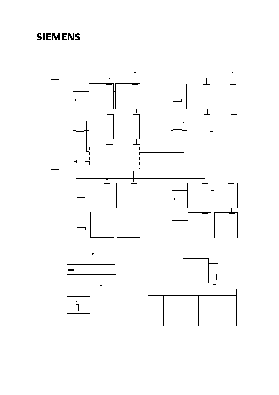
Block Diagram for 4M x 64/72 SDRAM DIMM modules (HYS64/72V4220GU)
CS
DQM
DQ0-DQ7
D1
CS
DQM
DQ0-DQ7
D0
CS
DQM
DQ0-DQ7
D16
CS
DQM
DQ0-DQ7
D2
CS
DQM
DQ0-DQ7
D3
CS1
CS0
DQMB0
DQ(7:0)
DQMB1
DQ(15:8)
CB(7:0)
DQMB2
DQ(23:16)
DQMB3
DQ(31:24)
A0-A10,BA
VDD
VSS
D0 - D15,(D16,D17)
C0-C31,(C32..C35)
E
2
PROM (256wordx8bit)
D0 - D15,(D16,D17)
D0 - D7,(D8)
D0 - D15,(D16,D17)
D0 - D7,(D16)
RAS, CAS, WE
CKE0
Note: D16 & D17 is only used in the x72 ECC version and all resistor values are 10 Ohms except otherwise noted.
CS2
CS
DQM
DQ0-DQ7
D9
CS
DQM
DQ0-DQ7
D8
CS
DQM
DQ0-DQ7
D17
CS
DQM
DQ0-DQ7
D10
CS
DQM
DQ0-DQ7
D11
CS
DQM
DQ0-DQ7
D5
CS
DQM
DQ0-DQ7
D4
CS
DQM
DQ0-DQ7
D6
CS
DQM
DQ0-DQ7
D7
DQMB4
DQ(39:32)
DQMB5
DQ(47:40)
DQMB6
DQ(55:48)
DQMB7
DQ(63:56)
CS
DQM
DQ0-DQ7
D13
CS
DQM
DQ0-DQ7
D12
CS
DQM
DQ0-DQ7
D14
CS
DQM
DQ0-DQ7
D15
CS3
D9 - D15,(D17)
CKE1
VDD
10k
WP
SDA
SA0
SA1
SA2
SA0
SA1
SA2
47k
Clock Wiring
CLK0 4 SDRAM+3.3pF 5 SDRAM
CLK1 4 SDRAM+3.3pF 5 SDRAM
CLK2 4 SDRAM+3.3pF 4 SDRAM+3.3pF
CLK3 4 SDRAM+3.3pF 4 SDRAM+3.3pF
4M x 64 4M x 72
SCL
SCL