 | –≠–ª–µ–∫—Ç—Ä–æ–Ω–Ω—ã–π –∫–æ–º–ø–æ–Ω–µ–Ω—Ç: ILD620B | –°–∫–∞—á–∞—Ç—å:  PDF PDF  ZIP ZIP |
5≠1
FEATURES
∑ Identical Channel to Channel Footprint
ILD620 Crosses to TLP620-2
ILQ620 Crosses to TLP620-4
∑ Current Transfer Ratio (CTR) at I
F
=
±
5 mA
ILD/Q620: 50% Min.
ILD/Q620GB: 100% Min.
∑ Saturated Current Transfer Ratio (CTR
SAT
)
at I
F
=
±
1 mA
ILD/Q620: 60% Typ.
ILD/Q620GB: 30% Min.
∑ High Collector-Emitter Voltage, BV
CEO
=70 V
∑ Dual and Quad Packages Feature:
- Reduced Board Space
- Lower Pin and Parts Count
- Better Channel to Channel CTR Match
- Improved Common Mode Rejection
∑ Field-Effect Stable by TRIOS
(TR
ansparent
IO
n
S
hield
)
∑ Isolation Test Voltage from Double Molded
Package
∑ Underwriters Lab File #E52744
∑ VDE 0884 Available with Option 1
Maximum Ratings
(Each Channel)
Emitter
Forward Current .........................................
±
60 mA
Surge Current...............................................
±
1.5 A
Power Dissipation ...................................... 100 mW
Derate from 25
∞
C .................................. 1.3 mW/
∞
C
Detector
Collector-Emitter Breakdown Voltage ............. 70 V
Collector Current.......................................... 50 mA
Collector Current (t <1 ms) ......................... 100 mA
Power Dissipation ...................................... 150 mW
Derate from 25
∞
C ..................................... 2 mW/
∞
C
Package
Isolation Test Voltage(t=1 sec.)......... 5300 VAC
RMS
Package Dissipation, ILD620/GB ............. 400 mW
Derate from 25
∞
C ............................... 5.33 mW/
∞
C
Package Dissipation, ILQ620/GB ............. 500 mW
Derate from 25
∞
C ............................... 6.67 mW/
∞
C
Creepage ................................................7 mm min.
Clearance ...............................................7 mm min.
Isolation Resistance
V
IO
=500 V, T
A
=25
∞
C ................................
10
12
V
IO
=500 V, T
A
=100
∞
C .............................
10
11
Storage Temperature .................. ≠55
∞
C to +150
∞
C
Operating Temperature............... ≠55
∞
C to +100
∞
C
Junction Temperature ................................... 100
∞
C
Soldering Temperature
(2 mm from case bottom).......................... 260
∞
C
DESCRIPTION
The ILD/Q620 and ILD/Q620GB are multi-channel input phototran-sistor
optocouplers that use inverse parallel GaAs IRLED emitters and high gain
NPN silicon phototransistors per channel. These devices are constructed
using over/under leadframe optical coupling and double molded insulation
resulting in a Withstand Test Voltage of 7500 VAC
PEAK
.
The LED parameters and the linear CTR characteristics combined with
the
TRIOS field-effect process make these devices well suited for AC voltage
detection. The ILD/Q620GB with its low IF guaranteed CTR
CEsat
minimizes
power dissipation of the AC
voltage detection network that is placed in
series with the LEDs. Eliminating the phototransistor base connection pro-
vides added electrical noise immunity from the transients found in many
industrial control environments.
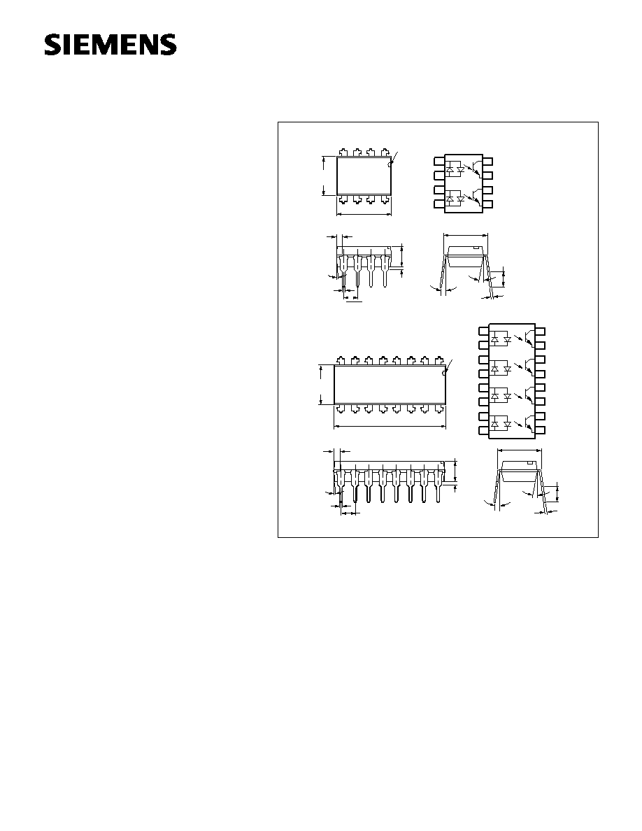
Dimensions in inches (mm)
.790 (20.07)
.779 (19.77 )
Pin One I.D.
Pin One I.D.
.268 (6.81)
.255 (6.48)
.268 (6.81)
.255 (6.48)
.268 (6.81)
.255 (6.48)
3
4
6
5
.390 (9.91)
.379 (9.63)
.045 (1.14)
.030 (.76)
4
∞
Typ.
.100 (2.54) Typ.
10
∞
Typ.
3
∞
≠9
∞
.305 Typ.
(7.75) Typ.
.022 (.56)
.018 (.46)
.012 (.30)
.008 (.20)
.135 (3.43)
.115 (2.92)
1
2
8
7
.150 (3.81)
.130 (3.30)
.040 (1.02)
.030 (.76 )
10
∞
Typ.
3
∞
≠9
∞
.305 Typ.
(7.75) Typ.
.012 (.30)
.008 (.20)
.135 (3.43)
.115 (2.92)
.045 (1.14)
.030 (.76)
4
∞
Typ.
.100 (2.54) Typ.
.022 (.56)
.018 (.46)
.150 (3.81)
.130 (3.30)
.040 (1.02)
.030 (.76 )
Collector
Emitter
Collector
Emitter
Collector
Emitter
Collector
Emitter
A/K
A/K
A/K
A/K
A/K
A/K
A/K
A/K
1
2
3
4
5
6
7
8
16
15
14
13
Collector
Emitter
Collector
Emitter
A/K
A/K
A/K
A/K
1
2
3
4
8
7
6
5
12
11
10
9
K=Cathode
K=Cathode
DUAL CHANNEL
ILD620/620GB
QUAD CHANNEL
ILQ620/620GB
AC INPUT PHOTOTRANSISTOR
OPTOCOUPLER
5≠2
ILD/Q620/GB
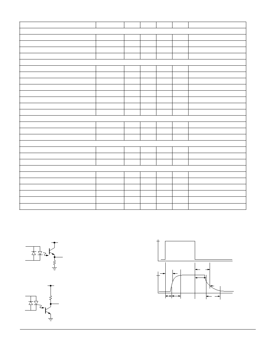
Characteristics
Symbol
Min.
Typ.
Max.
Unit
Condition
Emitter
Forward Voltage
V
F
1
1.15
1.3
V
I
F
=
±
10 mA
Forward Current
I
F
2.5
20
µ
A
V
R
=
±
0.7 V
Capacitance
C
O
25
pF
V
F
=0 V, f=1 MHz
Thermal Resistance, Junction to Lead
R
THJL
750
∞
C/W
Detector
Capacitance
C
CE
6.8
pF
V
CE
=5 V, f=1 MHz
Collector-Emitter Leakage Current
I
CEO
10
100
nA
V
CE
=24 V
Collector-Emitter Leakage Current
I
CEO
2
50
µ
A
T
A
=85
∞
C, V
CE
=24 V
Thermal Resistance, Junction to Lead
R
THJL
500
∞
C/W
Package Transfer Characteristics
Channel/Channel CTR Match
CTRX/CTRY
1 to 1
3 to 1
I
F
=
±
5 mA, V
CE
=5 V
CTR Symmetry
I
CE(RATIO)
0.5
2
I
CE
(I
F
=≠5 mA)/I
F
(=+5 mA)
Off-State Collector Current
I
CE(OFF)
1
10
µ
A
V
F
=
±
0.7 V, V
CE
=24 V
ILD/Q620
Saturated Current Transfer Ratio
CTR
CEsat
60
%
I
F
=
±
1 mA, V
CE
=0.4 V
Current Transfer Ratio
CTR
CE
50
80
600
%
I
F
=
±
5 mA, V
CE
=5 V
Collector-Emitter Saturation Voltage
V
CEsat
0.4
V
I
F
=
±
8 mA, I
CE
=2.4 mA
ILD/Q620GB
Saturated Current Transfer Ratio
CTR
CEsat
30
%
I
F
=
±
1 mA, V
CE
=0.4 V
Current Transfer Ratio (Collector-Emitter)
CTR
CE
100
200
600
%
I
F
=
±
5 mA, V
CE
=5 V
Collector-Emitter Saturation Voltage
V
CEsat
0.4
V
I
F
=
±
1 mA, I
CE
=0.2 mA
Isolation and Insulation
Common Mode Rejection, Output High
CMH
5000
V/
µ
s
V
CM
=50 V
P-P
, R
L
=1 k
, I
F
=0 mA
Common Mode Rejection, Output Low
CML
5000
V/
µ
s
V
CM
=50 V
P-P
, R
L
=1 k
, I
F
=10 mA
Common Mode Coupling Capacitance
C
CM
0.01
pF
Package Capacitance
CI-O
0.8
pF
V
I-O
=0 V, f=1 MHz
Insulation Resistance
R
S
10
12
V
I-O
=500 V
Channel to Channel Insulation
500
VAC
Switching Times
Figure 1. Non-saturated switching timing
Figure 2. Saturated switching timing
V
O
V
CC
=5 V
R
L
=75
F=10 KHz,
DF=50%
I
F
=10 mA
V
O
V
CC
=5 V
R
L
F=10 KHz,
DF=50%
I
F
=10 mA
Figure 3. Non-saturated switching timing
V
0
I
F
t
PHL
t
S
t
R
t
F
t
D
50%
t
PLH
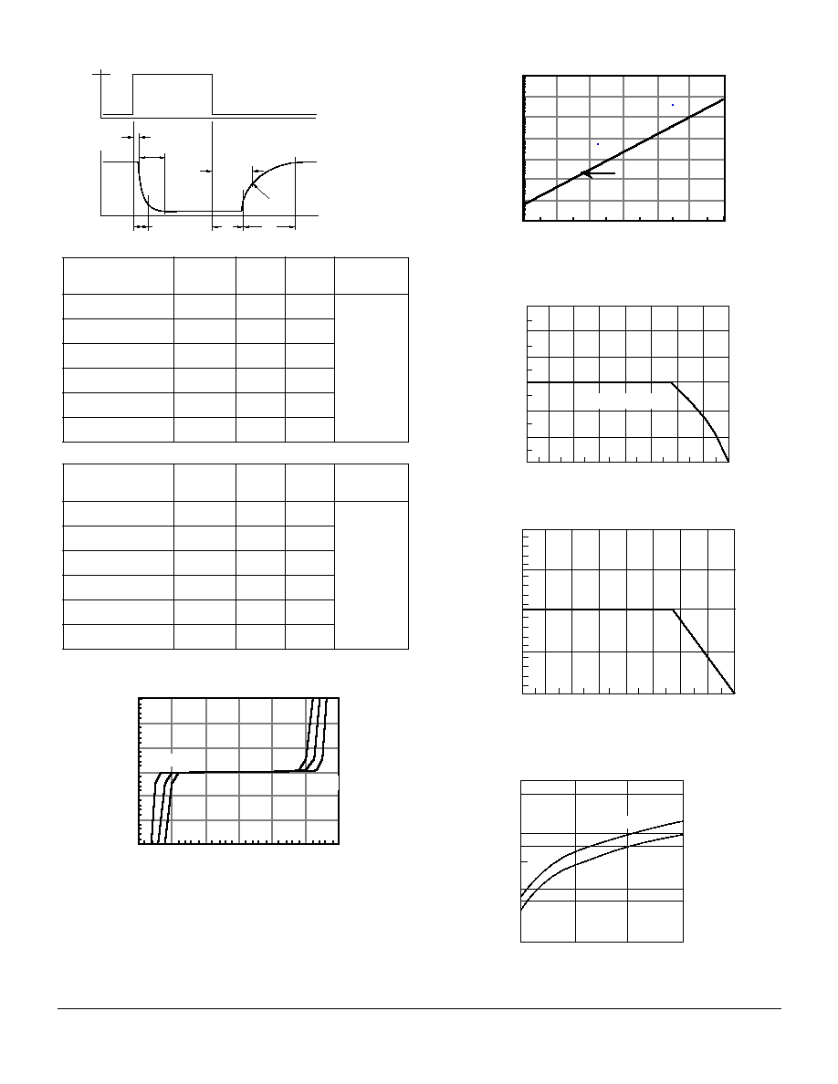
5≠3
ILD/Q620/GB
Figure 4. Saturated switching timing
Figure 5. LED forward current versus forward voltage
Characteristic
Symbol
Typ.
Unit
Test
Condition
On Time
T
ON
3.0
µ
s
I
F
=
±
10 mA
V
CC
=5 V
R
L
=75
50% of V
PP
Rise Time
t
R
20
µ
s
Off Time
t
OFF
2.3
µ
s
Fall Time
t
F
2.0
µ
s
Propagation H-L
t
PHL
1.1
µ
s
Propagation L-H
t
PLH
2.5
µ
s
Characteristic
Symbol
Typ.
Unit
Test
Condition
On Time
T
ON
4.3
µ
s
I
F
=
±
10 mA
V
CC
=5 V
R
L
=1
V
TH
=1.5 V
Rise Time
t
R
2.8
µ
s
Off Time
t
OFF
2.5
µ
s
Fall Time
t
F
11
µ
s
Propagation H-L
t
PHL
2.6
µ
s
Propagation L-H
t
PLH
7.2
µ
s
I
F
t
R
V
O
t
D
t
S
t
F
t
PHL
t
PLH
V
TH
=1.5 V
-1.5
-1.0
-0.5
0.0
0.5
1.0
1.5
-60
-40
-20
0
20
40
60
25
∞
C
85
∞
C
≠55
∞
C
VF - LED Forward Voltage - V
IF - LED Forward Current - mA
Figure 6. Collector-emitter leakage versus temperature
Figure 7. Maximum LED current versus ambient
temperature
Figure 8. Maximum LED power dissipation
Figure 9. Collector current versus diode forward
current
100
80
60
40
20
0
-20
10
10
10
10
10
10
10
10
-2
-1
0
1
2
3
4
5
g
p
Ta - Ambient Temperature -
∞
C
Iceo - Collector-Emitter - nA
TYPICAL
Vce = 10V
--60 -40 -20 0 20 40 60 80 100
120
100
80
60
40
0
20
Ta - Ambient Temperature -
∞
C
IF - Maximum LED Current - mA
TJ (MAX)=100
∞
C
--60 -40 -20 0 20 40 60 80 100
200
100
0
50
Ta - Ambient Temperature -
∞
C
P
LED
- LED Power - mW
150
1 5 10 20
100
50
10
2.5
5.0
1.0
0.5
0.1
Forward Current≠I
F
(mA)
I
C
≠Normalized Collector Current
Normalized to
ILD/Q620GB
ILD/Q620
I
F
=10 mA
V
CE
=5 V
T
A
=25
∞
C
5≠4
ILD/Q620/GB
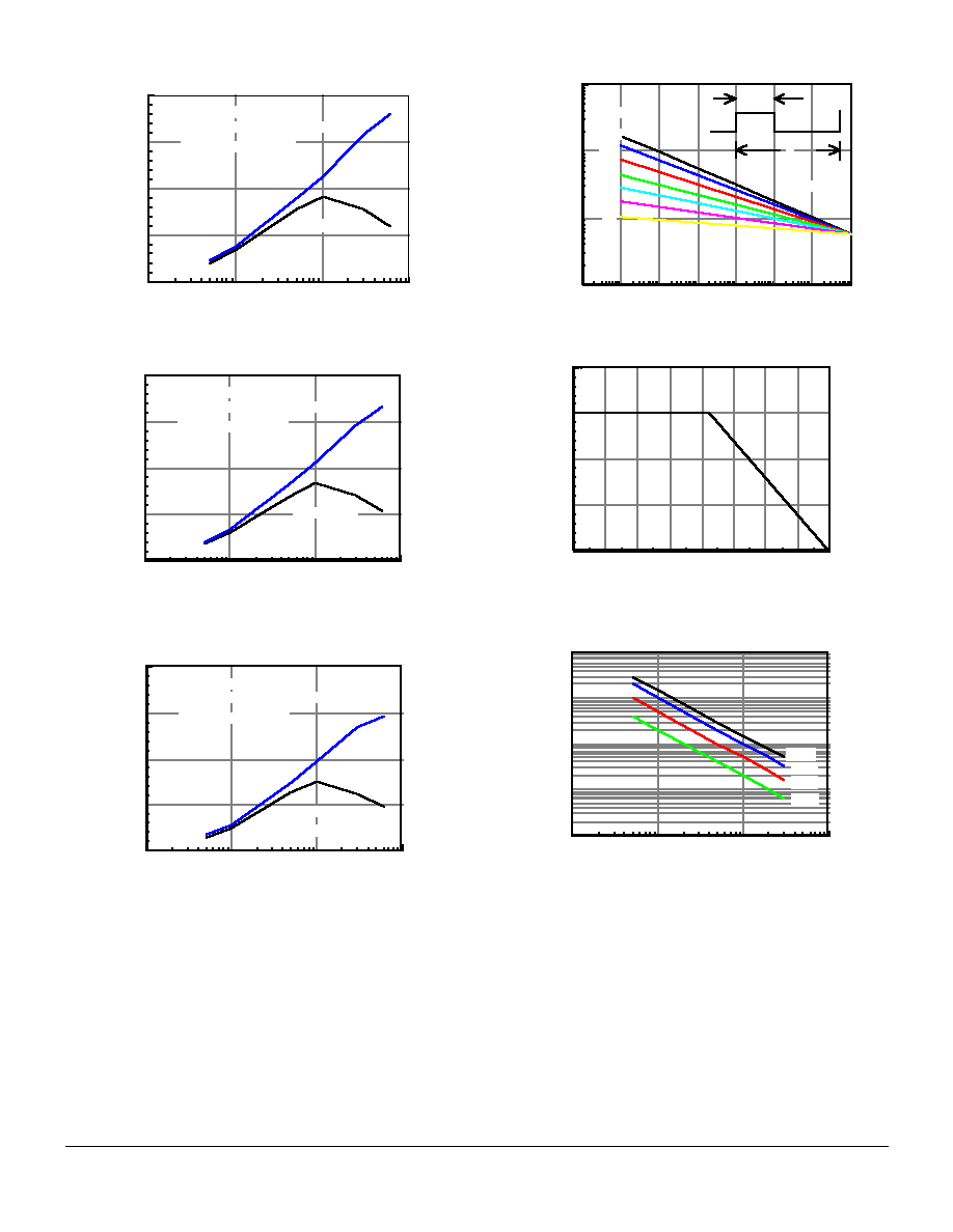
Figure 10. Normalization factor for non-saturated and
saturated CTR T
A
=50
∞
C versus if
Figure 11. Normalization factor for non-saturated and
saturated CTR T
A
=70
∞
C versus if
Figure 12. Normalization factor for non-saturated and
saturated CTR T
A
=100
∞
C versus if
.1
1
10
100
0.0
0.5
1.0
1.5
2.0
Normalized to:
Vce = 10V, IF = 5mA, Ta = 25
∞
C
Ta = 50
∞
C
CTRce(sat) Vce = 0.4V
CTRNF - Normalized CTR Factor
IF - LED Current - mA
NCTRce(sat)
NCTRce
.1
1
10
100
0.0
0.5
1.0
1.5
2.0
Normalized to:
Vce = 10V, IF = 5mA, Ta = 25
∞
C
Ta = 70
∞
C
CTRce(sat) Vce = 0.4V
CTRNF - Normalized CTR Factor
IF - LED Current - mA
NCTRce(sat)
NCTRce
.1
1
10
100
0.0
0.5
1.0
1.5
2.0
Normalized to:
Vce = 10V, IF = 5mA, Ta = 25
∞
C
Ta = 100
∞
C
CTRce(sat) Vce = 0.4V
CTRNF - Normalized CTR Factor
IF - LED Current - mA
NCTRce(sat)
NCTRce
Figure 13. Peak LED current versus peak duration, Tau
Figure 14. Maximum detector power dissipation
Figure 15. Maximum collector current versus collector
voltage
10-6
10-5
10-4
10-3
10-2
10-1
10 0
10 1
10
100
1000
10000
t - LED Pulse Duration - s
If(pk) - Peak LED Current - mA
.005
.05
.02
.01
.1
.2
.5
Duty Factor
t
DF = /t
-60
-40
-20
0
20
40
60
80
100
0
50
100
150
200
Ta - Ambient Temperature -
∞
C
P - Detector Power - mW
DET
.1
1
10
100
.1
1
10
100
1000
Vce - Collector-Emitter Voltage - V
Ice - Collector Current - mA
25
∞
C
50
∞
C
75
∞
C
90
∞
C
Rth = 500
∞
C/W