Semiconductor Group
1
1998-11-16
LPT 80 A
Typ
Type
Bestellnummer
Ordering Code
Geh‰use
Package
LPT 80 A
Q68000-A7852
Klares Kunststoffgeh‰use, Lˆtspieþe im 2.54-mm-Raster
(
1
/
10
"), Kollektorkennzeichnung: L‰ngerer Lˆtspieþ
Clear plastic miniature package, 2.54 mm (
1
/
10
") lead spacing,
collector marking: long solder lead
NPN-Silizium-Fototransistor
Silicon NPN Phototransistor
Wesentliche Merkmale
q
Speziell geeignet f¸r Anwendungen im
Bereich von 470 nm bis 1080 nm
q
Sidelooker im Kunststoffgeh‰use
q
Hohe Empfindlichkeit
q
Passend zu IRED IRL 80 A, IRL 81 A
Anwendungen
q
Fertigungs- und Kontrollanwendungen der
Industrie
q
Lichtschranken
Features
q
Especially suitable for applications from
470 nm to 1080 nm
q
Sidelooker in plastic package
q
High sensitivity
q
Matches IR emitter IRL 80 A, IRL 81 A
Applications
q
A variety of manufacturing and monitoring
applications
q
Photointerrupters
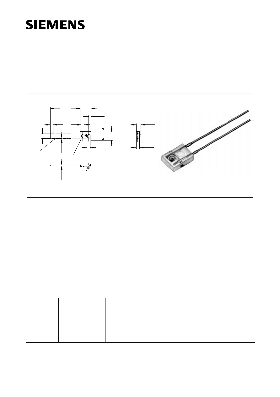
LPT 80 A
Maþe in mm, wenn nicht anders angegeben/Dimensions in mm, unless otherwise specified
16.51
16.00
5.84
5.59
1.29
1.14
1.52
1.52
1.52
2.54mm
spacing
0.64
0.46
2.34
2.08
4.57
4.32
2.54
2.03
1.70
1.45
0.64
0.46
R = 0.76
Approx. weight 0.2 g
Collector
Plastic marking
GEO06391
feo06391

Semiconductor Group
2
1998-11-16
LPT 80 A
Grenzwerte
Maximum Ratings
Bezeichnung
Description
Symbol
Symbol
Wert
Value
Einheit
Unit
Betriebs- und Lagertemperatur
Operating and storage temperature range
T
op
;
T
stg
≠ 40 ... + 100
∞
C
Kollektor-Emitterspannung
Collector-emitter voltage
V
CE
30
V
Kollektorstrom
Collector current
I
C
50
mA
Kollektorspitzenstrom,
=
10
µ
s
Collector surge current
I
CS
100
mA
Emitter-Kollektorspannung
Emitter-collector voltage
V
EC
7
V
Verlustleistung,
T
A
= 25
∞
C
Total power dissipation
P
tot
100
mW
W‰rmewiderstand
Thermal resistance
R
thJA
750
K/W
Semiconductor Group
3
1998-11-16
LPT 80 A
Kennwerte (
T
A
= 25
∞
C,
= 950 nm)
Characteristics
Bezeichnung
Description
Symbol
Symbol
Wert
Value
Einheit
Unit
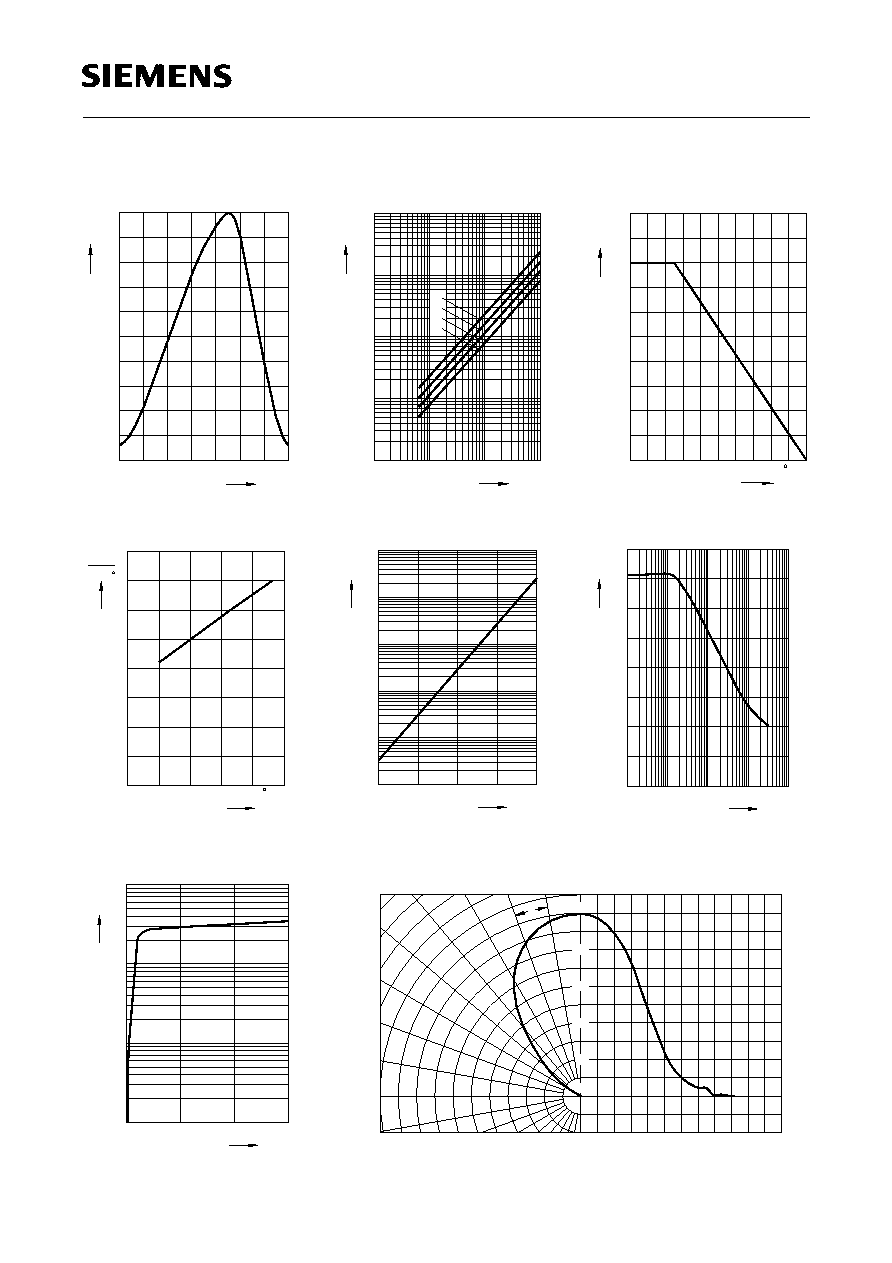
Wellenl‰nge der max. Fotoempfindlichkeit
Wavelength of max. sensitivity
S max
850
nm
Spektraler Bereich der Fotoempfindlichkeit
S=10% von Smax
Spectral range of sensitivity
S=10% of Smax
430 ... 1070
nm
Abmessung der Chip-Fl‰che
Dimensions of chip area
L
x
B
L
x
W
0.55 x 0.55
mm x mm
Halbwinkel
Half angle
±
35
Grad
deg.
Kapazi‰t,
V
CE
= 5 V,
f
= 1 MHz,
E
= 0
Capacitance
C
CE
3.3
pF
Dunkelstrom,
V
CE
= 5 V
Dark current
I
R
3 (< 50)
nA
Bezeichnung
Description
Symbol
Symbol
Wert
Value
Einheit
Unit
Fotostrom
Photocurrent
E
e
= 0.5 mW/cm
2
,
V
CE
= 5 V,
= 950 nm
E
v
= 1000 lx, Normlicht/standard light A,
V
CE
= 5 V
I
PCE
I
PCE
> 0.25
3.2
mA
Anstiegs- und Abfallzeit
Rise and fall time
R
L
= 1 k
,
V
= 5 V,
=950 nm,
I
C
= 1 mA
t
r
,
t
f
10
µ
s
Kollektor-Emitter-S‰ttigungsspannung
Collector-emitter saturation voltage
I
C
=
I
PCE min
x 0.8,
E
e
= 0.5 mW/cm
2
V
CEsat
150
mV