CGY 81
Siemens Aktiengesellschaft
1
23.07.98
HL HF PE GaAs 1/Fo
GaAs MMIC
l
Tri mode power amplifier for AMPS/ CDMA /TDMA
portable cellular phones
l
31 dBm saturated output power @ PAE=55% typ.
29 dBm linear output power@ PAE=40% typ.
l
Fully integrated 2 stage amplifier
l
Power ramp control
l
Input matched to 50 ohms, simple output match
ESD: Electrostatic discharge sensitive device,
observe handling precautions!
Type
Marking
Ordering code
(taped)
Package
CGY 81
CGY 81
Q627002G0078
MW 16
Maximum Ratings
Characteristics
Symbol
max. Value
Unit
Positive supply voltage
VD
9
V
Supply current
ID
4
A
Channel temperature
TCh
150
�C
Storage temperature
Tstg
-55...+150
�C
Pulse peak power dissipation
PPulse
tbd
W
Total power dissipation
(Ts
80 �C)
Ts: Temperature at soldering point
Ptot
Tbd
W
Thermal Resistance
Characteristics
Symbol
max. Value
Unit
Channel-soldering point
RthChS
11
K/W
Semiconductor Group
1
1998-11-01
CGY 81
Siemens Aktiengesellschaft
2
23.07.98
HL HF PE GaAs 1/Fo
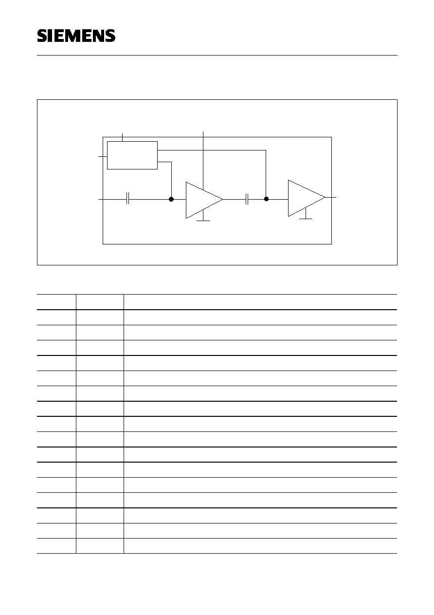
Functional Block Diagram:
Pin Configuration:
Pin #
Name
Configuration
1
VD Cell
Drain voltage preamplifier stage
2
n. c.
3
RF IN Cell RF IN
4
n. c.
5
Vneg
Negative voltage
6
Vcon
Control voltage
7
n. c.
8
n. c.
9
n. c.
10
n. c.
11
RF out
RF out / drain voltage final stage
12
RF out
RF out / drain voltage final stage
13
RF out
RF out / drain voltage final stage
14
RF out
RF out / drain voltage final stage
15
n. c.
16
n. c.
RF OUT
VD1
RF IN
Vcon
Control
Circuit
Vneg
Semiconductor Group
2
1998-11-01
CGY 81
Siemens Aktiengesellschaft
3
23.07.98
HL HF PE GaAs 1/Fo
Electrical Characteristics
(TA = 25�C , ZS=ZL=50 Ohm, VD=3.5V, Idq=300mA, unless otherwise specified )
Characteristics
Symbol
min
typ
max
Unit
Frequency range
f
824
849
MHz
Duty cycle
t
ON
/t
OFF
100
%
AMPS output power
P
31,5
dBm
TDMA output power
P
30
dBm
AMPS gain at max. output
G
24
dB
TDMA gain at max. output
G
27
dB
CDMA output power
P
28
dBm
CDMA gain at max. output
G
28
dB
Power ramping characteristic
Full output power
Pinch off
V
contr
2.5
0.5
V
Adjacent Channel Power CDMA
900kHz offset
1.98 MHz offset
P
adj
/P
main
-45
-54
dBc @
30kHz
Adjacent channel power TDMA
adjacent
alternate
2nd alternate
P
adj
/P
main
-28
�45
-45
dBc @
30kHz
AMPS efficiency
PAE
55
%
TDMA DC to RF efficiency
@Padj=-26dBc
at max. output
PAE
40
%
CDMA DC to RF efficiency
@Padj=-42dBc
at max. output
at Pout=10 dBm ( Iq set to 100mA )
PAE
35
8
%
Receive band noise power density
( 869 to 894 MHz )
P
RX
-137
dBm/Hz
Drain supply voltage range
VD
2.7
3.5
4.0
V
Negative supply voltage range
Vneg
-5.0
-7
V
Standby current @Vcon=0V
I
pwr dwn
500
�
A
Quiescent current
I
Q
300
mA
Current consumption at V
Contr
I
Control
2
mA
Current consumption at V
NEG
I
NEG
2
mA
Operating temperature range
-30
+85
�C
Semiconductor Group
3
1998-11-01
CGY 81
Siemens Aktiengesellschaft
4
23.07.98
HL HF PE GaAs 1/Fo
Power on sequence:
1. connect negative voltage to PA
2. connect control voltage to PA
3. turn on Vd
4. turn on Pin
To switch off the device please use reverse sequence.
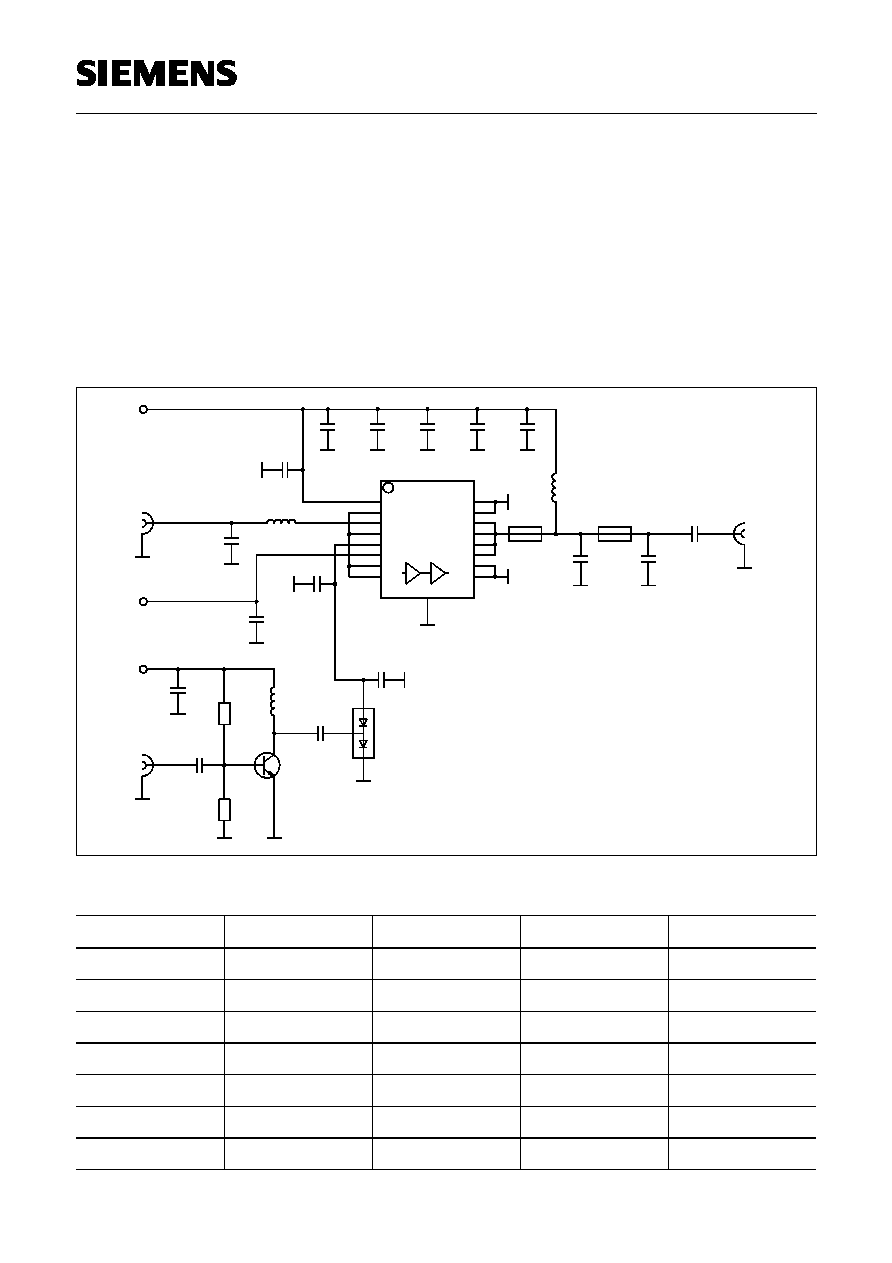
Application Circuit:
Evaluation Board Parts List
Part Type
Position
Description
Manufacturer
Part Number
Capacitor
C1
3.9pF 0402
Siemens
Capacitor
C2, C7, C10
100pF 0402
Siemens
Capacitor
C3, C4, C5, C6
1uF 1206
Siemens
Capacitor
C8
5.6pF 0603 HQ
AVX
06035J5R6GBT
Capacitor
C9
10pF 0603 HQ
AVX
06035J100GBT
Capacitor
C11, C12
10 nF 0402
Siemens
Capacitor
C13, C15
1 nF 0402
Siemens
C
9
1
0
p
H
Q
C
8
5
p
6
H
Q
1
u
0
C
6
C
5
1
u
0
1
u
0
C
4
C
3
1
u
0
L3
8n2
L
2
3
3
n
H
L
1
1
0
u
H
RFout
CLK
RFin
BC848B
V2
BAS 40-04
V1
3
2
1
CGY81
IC1
1
VD1
5
Vneg
14
VD2/RFout4
13
VD2/RFout3
12
VD2/RFout2
6
Vcon
3
RFin
16
NC16
15
NC15
10
NC10
9
NC9
8
NC8
7
NC7
4
NC4
2
NC2
17
GND (backside MW16)
11
VD2/RFout1
C16
33n
Vaux
Vcon
Vd
R
1
3
k
9
R
2
6
8
0
R
C15
1n0
3
3
n
C
1
4
C13
1n0
10n
C12
C
1
1
1
0
n
C10
100p
C
7
1
0
0
p
C2
100p
C
1
3
p
9
Semiconductor Group
4
1998-11-01
CGY 81
Siemens Aktiengesellschaft
5
23.07.98
HL HF PE GaAs 1/Fo
Part Type
Position
Description
Manufacturer
Part Number
Capacitor
C14, C16
33nF 0402
Siemens
Inductor
L1
10uH
Siemens
Inductor
L2
33nH Air Coil
H. David GmbH
PN/BV 1250
Inductor
L3
8.2nH 0603
Resistor
R1
3.9k 0402
Resistor
R2
680 Ohm 0402
Diode
V1
BAS40-04W
Siemens
Transistor
V2
BC848B
Siemens
Substrate
FR4, h=0.2mm,
r
=4.5
Siemens
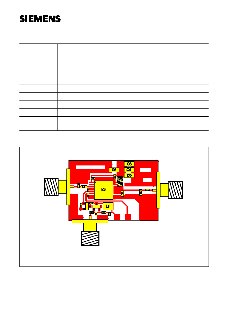
Evaluation Board:
RFin
Vd
SIEMENS
RFout
CGY 81 Cell Band PA
Vaux
Vcon
CLK
L2
R
F
o
u
t
CLK
R
F
i
n
V
2
V1
Semiconductor Group
5
1998-11-01