BAV 99S
Semiconductor Group
Apr-27-1998
1
Silicon Switching Diode Array
∑
For high-speed switching applications
∑
Connected in series
∑
Internal (galvanic) isolated Diodes
in one package
VPS05604
6
3
1
5
4
2
Type
Marking Ordering Code
Package
Pin Configuration
A7s
Q62702-A1277
1/4 = A1 2/5 = C2 3/6=C1/A2 SOT-363
BAV 99S
Maximum Ratings
Parameter
Value
Symbol
Unit
V
V
R
70
Diode reverse voltage
Peak reverse voltage
V
RM
70
200
mA
Forward current
I
F
A
I
FS
Surge forward current, t = 1
µ
s
4.5
Total power dissipation,
T
S
= 85 ∞C
P
tot
250
mW
150
∞C
Junction temperature
T
j
Storage temperature
T
stg
65 ...+150
Thermal Resistance
K/W
Junction - ambient
1)
R
thJA
530
Junction - soldering point
R
thJS
260
1) Package mounted on epoxy pcb 40mm x 40mm x 1.5mm / 0.5cm2 Cu
Semiconductor Group
1
1998-11-01
BAV 99S
Semiconductor Group
Apr-27-1998
2
Electrical Characteristics at
T
A
= 25∞C, unless otherwise specified.
Parameter
Values
Symbol
Unit
max.
typ.
min.
DC characteristics
V
V
(BR)
Breakdown voltage
I
(BR)
= 100 µA
-
-
70
mV
Forward voltage
I
F
= 1 mA
I
F
= 10 mA
I
F
= 50 mA
I
F
= 150 mA
-
-
-
-
-
-
-
-
V
F
715
855
1000
1250
µA
Reverse current
V
R
= 70 V
I
R
2.5
-
-
nA
Reverse current
V
R
= 25 V,
T
A
= 150 ∞C
V
R
= 70 V,
T
A
= 150 ∞C
I
R
-
-
-
-
30
50
AC characteristics
pF
Diode capacitance
V
R
= 0 V,
f
= 1 MHz
-
1.5
-
C
D
Reverse recovery time
I
F
= 10 mA,
I
R
= 10 mA,
R
L
= 100
,
measured at
I
R
= 1mA
t
rr
6
ns
-
-
Test circuit for reverse recovery time
EHN00019
F
D.U.T.
Oscillograph
Pulse generator:
t
p
= 100ns,
D = 0.05,
t
r
= 0.6ns,
R
i
= 50
Oscillograph:
R = 50
,
t
r
= 0.35ns,
C
1pF
Semiconductor Group
2
1998-11-01
BAV 99S
Semiconductor Group
Apr-27-1998
3
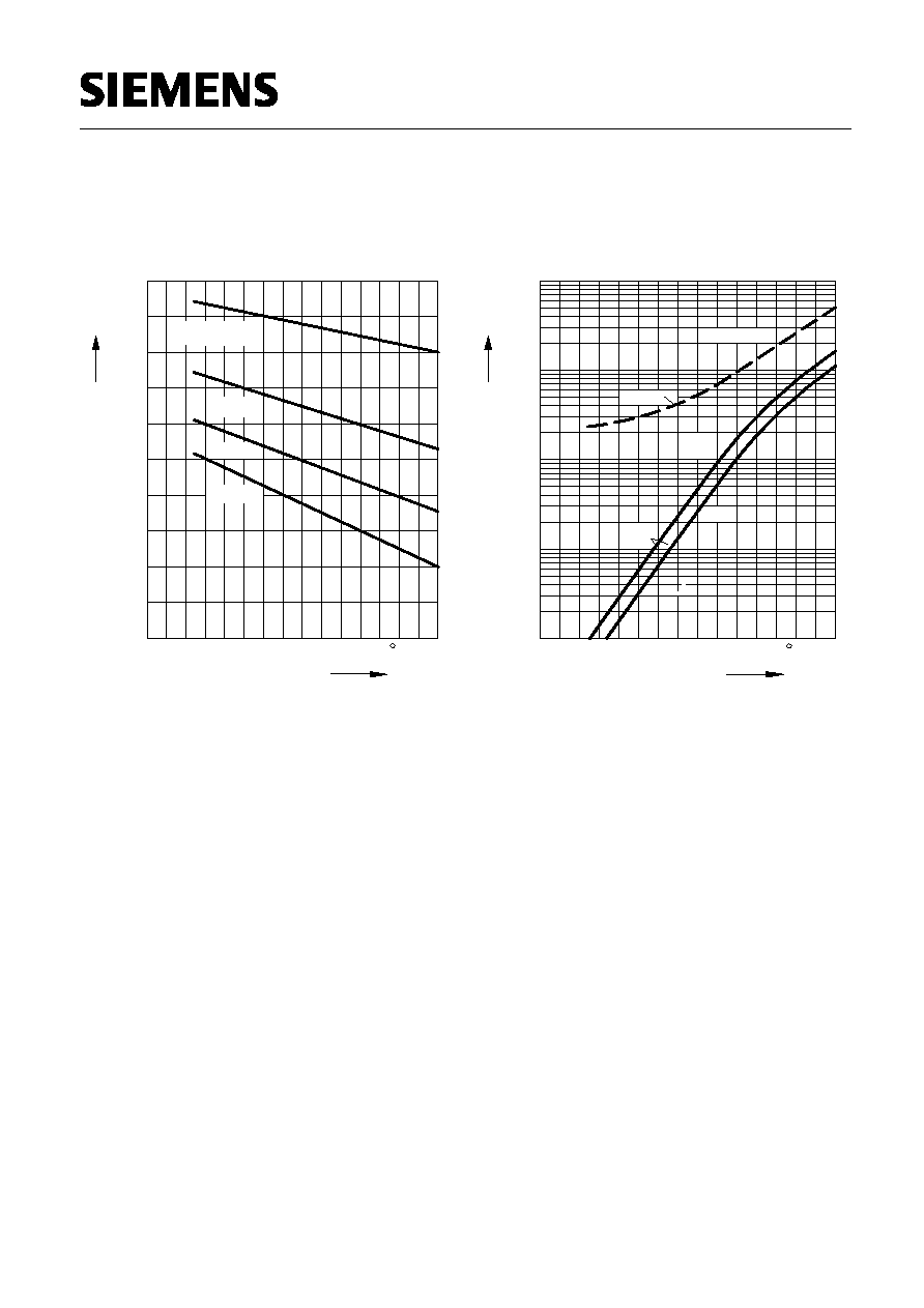
Forward current
I
F
=
f (T
A
*;
T
S
)
* Package mounted on epoxy
0
20
40
60
80
100
120 ∞C
150
T
A
,T
S
0
50
100
150
200
mA
300
I
F
1
T
S
T
A
Forward current
I
F
=
f V
F
)
T
A
= 25∞C
EHB00076
BAV 99
F
150
mA
100
50
0
V
F
1.5
V
1.0
0.5
0
typ
max
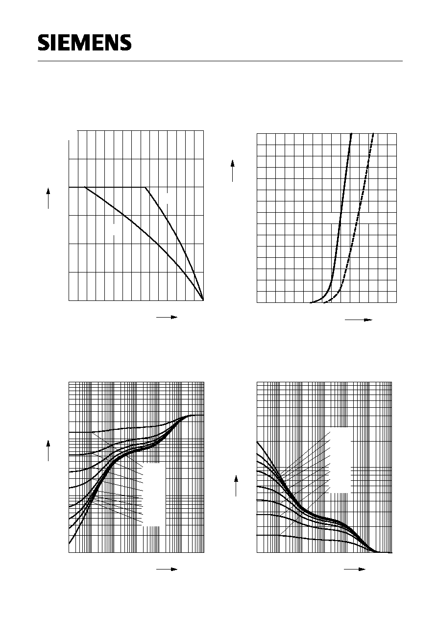
Permissible Pulse Load
R
thJS
=
f(t
p
)
10
-6
10
-5
10
-4
10
-3
10
-2
10
0
s
t
p
0
10
1
10
2
10
3
10
K/W
R
thJS
0.5
0.2
0.1
0.05
0.02
0.01
0.005
D = 0
Permissible Pulse Load
I
Fmax
/
I
FDC
=
f(t
p
)
10
-6
10
-5
10
-4
10
-3
10
-2
10
0
s
t
p
0
10
1
10
2
10
-
I
Fmax
/
I
FDC
D = 0
0.005
0.01
0.02
0.05
0.1
0.2
0.5
Semiconductor Group
3
1998-11-01