
BAS 70-06S
Semiconductor Group
Sep-07-1998
1
Silicon Schottky Diode Array
∑
General-purpose diode for high-speed switching
∑
Circuit protection
∑
Voltage clamping
∑
High-level detecting and mixing
∑
Available with CECC quality assessment
VPS05604
6
3
1
5
4
2
Type
Marking Ordering Code
Pin Configuration
Package
BAS 70-06S
76s
Q62702-A3469
1/4=C1
2/5=C2
SOT-363
3/6=A1/A2
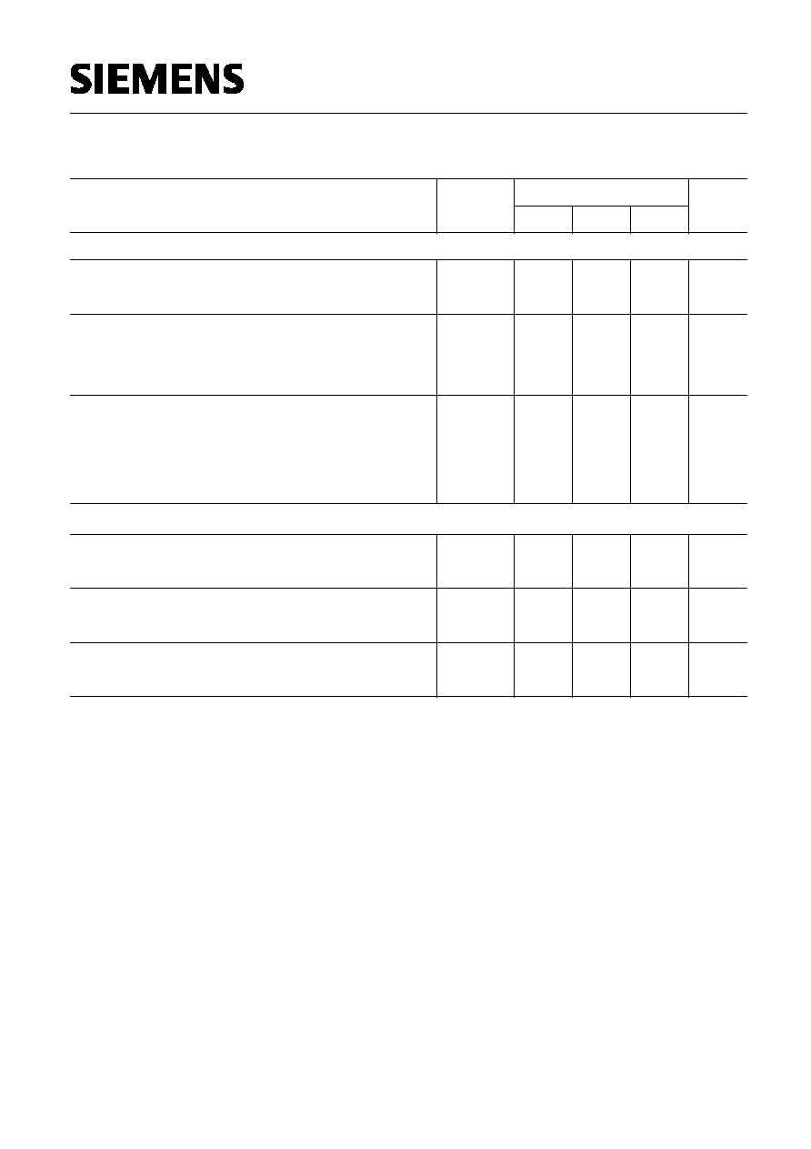
Maximum Ratings
Parameter
Symbol
Value
Unit
Diode reverse voltage
V
R
70
V
Forward current
I
F
70
mA
Surge forward current (t
<
100
µ
s)
I
FSM
100
Total power dissipation,
T
S
72 ∞C
P
tot
250
mW
Junction temperature
T
j
150
∞C
Operating temperature range
T
op
- 55 ...+150
Storage temperature
T
stg
- 55 ...+150
Thermal Resistance
Junction - ambient
1)
R
thJA
545
K/W
Junction - soldering point
R
thJS
310
1) Package mounted on epoxy pcb 40mm x 40mm x 1.5mm / 0.5cm 2 Cu
Semiconductor Group
1
1998-11-01
BAS 70-06S
Semiconductor Group
Sep-07-1998
2
Electrical Characteristics at
T
A
= 25∞C, unless otherwise specified.
Parameter
Symbol
Unit
Values
min.
max.
typ.
DC characteristics
Breakdown voltage
I
(BR)
= 10 µA
V
(BR)
70
V
-
-
I
R
-
-
-
-
0.1
10
Reverse current
V
R
= 50 V
V
R
= 70 V
µA
Forward voltage
I
F
= 1 mA
I
F
= 10 mA
I
F
= 15 mA
V
F
300
600
750
375
705
880
410
750
1000
mV
AC characteristics
Diode capacitance
V
R
= 0 V,
f = 1 MHz
C
T
-
1.6
2
pF
Charge carrier life time
I
F
= 25 mA
-
-
100
ps
Differential forward resistance
I
F
= 10 mA,
f = 100 MHz
r
f
-
30
-
Semiconductor Group
2
1998-11-01

BAS 70-06S
Semiconductor Group
Sep-07-1998
3
Forward current
I
F
=
f (T
A
*;
T
S
)
* Package mounted on epoxy
0
20
40
60
80
100
120 ∞C
150
T
A
,T
S
0
20
40
60
mA
100
I
F
T
S
T
A
Permissible Pulse Load
R
thJS
=
f(t
p
)
10
-7
10
-6
10
-5
10
-4
10
-3
10
-2
10
0
s
t
p
0
10
1
10
2
10
3
10
K/W
R
thJS
0.5
0.2
0.1
0.05
0.02
0.01
0.005
D = 0
Permissible Pulse Load
I
Fmax
/
I
FDC
=
f(t
p
)
10
-6
10
-5
10
-4
10
-3
10
-2
10
0
s
t
p
0
10
1
10
2
10
-
I
Fmax
/
I
FDC
D = 0
0.005
0.01
0.02
0.05
0.1
0.2
0.5
Semiconductor Group
3
1998-11-01
