Semiconductor Group
1
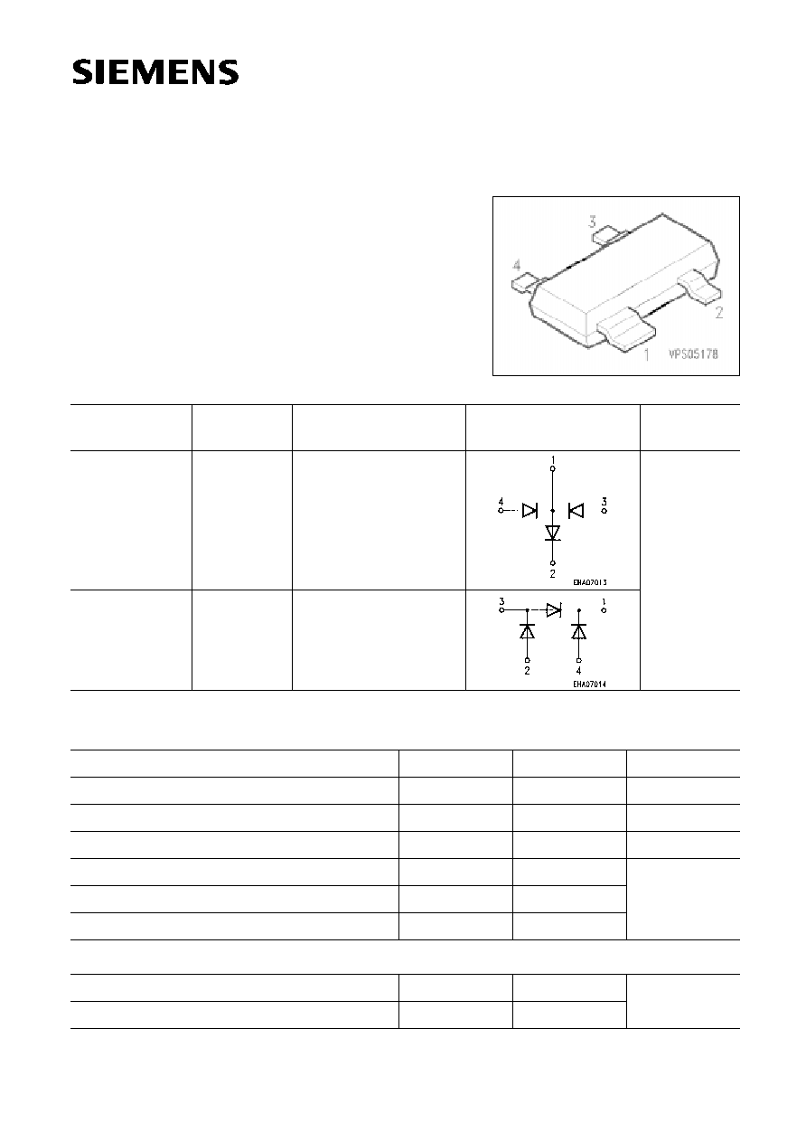
Silicon PIN Diodes
BAR 60
BAR 61
Maximum Ratings per Diode
Type
Ordering Code
(tape and reel)
Marking
Package
1)
Pin Configuration
BAR 60
Q62702-A786
60
SOT-143
BAR 61
Q62702-A120
61
Parameter
Symbol
Values
Unit
Reverse voltage
V
R
100
V
Total power dissipation,
T
S
65 �C
2)
P
tot
250
mW
T
j
150
�C
Forward current
I
F
140
mA
Junction temperature
Storage temperature range
T
op
� 55 ... + 150
T
stg
� 55 ... + 150
Thermal Resistance
Junction - ambient
2)
R
th JA
580
K/W
Junction - soldering point
R
th JS
340
Operating temperature range
1)
For detailed information see chapter Package Outlines.
2)
Package mounted on alumina 15 mm
�
16.7 mm
�
0.7 mm.
q
RF switch
q
RF attenuator for frequencies above 10 MHz
07.94

Semiconductor Group
2
BAR 60
BAR 61
BAR 60
Electrical Characteristics per Diode
at
T
A
= 25 �C, unless otherwise specified.
Unit
Values
Parameter
Symbol
min.
typ.
max.
DC/AC Characteristics
V
Forward voltage
I
F
= 100 mA
V
F
�
�
1.25
�
s
Charge carrier life time
I
F
= 10 mA,
I
R
= 6 mA
L
�
1
�
nA
�
A
Reverse current
V
R
= 50 V
V
R
= 100 V
I
R
�
�
�
�
100
1
�
S
Zero bias conductance
V
R
= 0,
f
= 100 MHz
g
p
�
50
�
pF
Diode capacitance
V
R
= 50 V,
f
= 1 MHz
V
R
= 0,
f
= 100 MHz
C
T
�
�
0.25
0.2
0.5
�
Differential forward resistance
f
= 100 MHz,
I
F
= 0.01 mA
I
F
= 0.1 mA
I
F
= 1.0 mA
I
F
= 10 mA
r
f
�
�
�
�
2800
380
45
7
�
�
�
�
Semiconductor Group
4
BAR 60
BAR 61
BAR 60
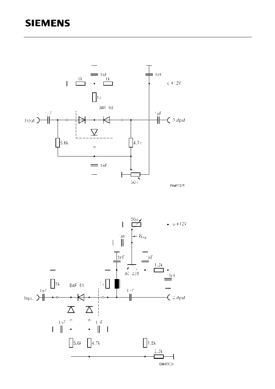
Application circuit for attenuation networks with diode BAR 60
Application circuit for attenuation networks with diode BAR 61
