Semiconductor Group
1
Silicon Switching Diodes
BAS 19
... BAS 21
Maximum Ratings
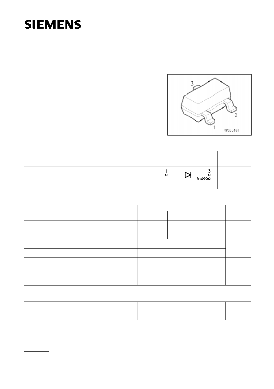
Type
Ordering Code
(tape and reel)
Marking
Package
1)
Pin Configuration
BAS 19
BAS 20
BAS 21
Q62702-A95
Q62702-A113
Q62702-A79
JPs
JRs
JSs
SOT-23
Parameter
Symbol
Values
BAS 19
BAS 20
BAS 21
Unit
Reverse voltage
V
R
V
Peak forward current
I
FM
Forward current
I
F
mA
Junction temperature
T
j
�C
Total power dissipation,
T
S
= 70 �C
P
tot
mW
Storage temperature range
T
stg
Peak reverse voltage
V
RM
100
150
200
120
200
250
250
625
350
150
� 65 ... + 150
Thermal Resistance
Junction - ambient
2)
R
th JA
K/W
Junction - soldering point
R
th JS
300
230
1)
For detailed information see chapter Package Outlines.
2)
Package mounted on epoxy pcb 40 mm
�
40 mm
�
1.5 mm/6 cm
2
Cu.
q
High-speed, high-voltage switch
07.94
Semiconductor Group
2
BAS 19
... BAS 21
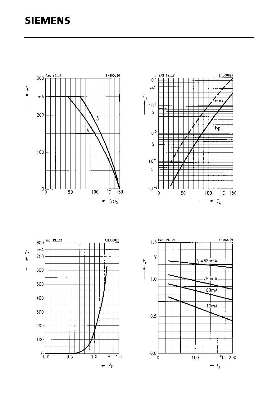
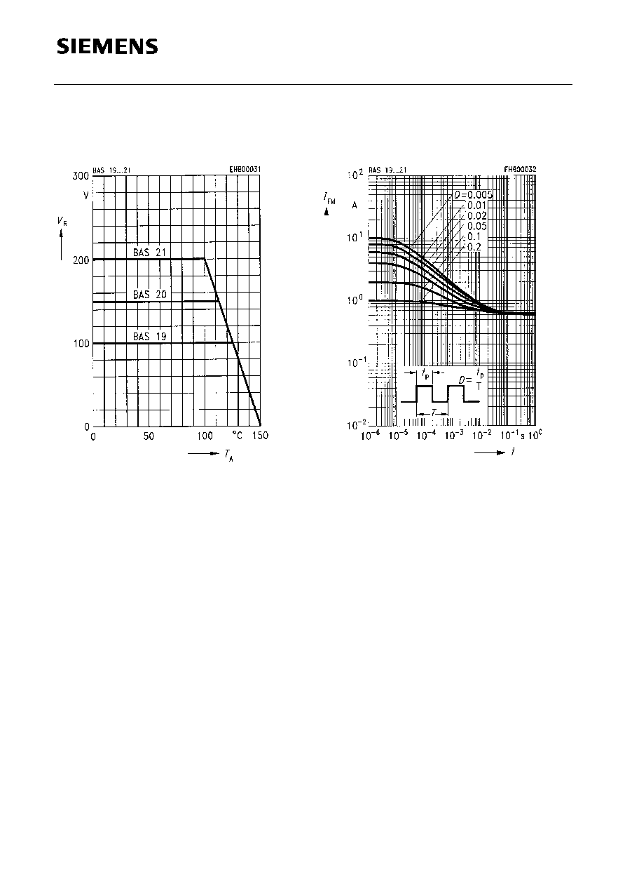
Electrical Characteristics
at
T
A
= 25 �C, unless otherwise specified.
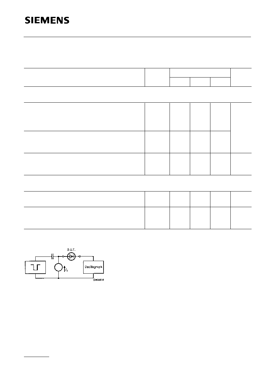
Test circuit for reverse recovery time
Pulse generator:
t
p
= 100 ns,
D
= 0.05
Oscillograph:
R
= 50
t
r
= 0.6 ns,
R
j
= 50
t
r
= 0.35 ns
C
1 pF
V
Breakdown voltage
1)
I
(BR)
= 100
�
A
BAS 19
BAS 20
BAS 21
V
(BR)
120
200
250
�
�
�
�
�
�
Forward voltage
I
F
= 100 mA
I
F
= 200 mA
V
F
�
�
�
�
1
1.25
nA
�
A
Reverse current
V
R
=
V
R max
V
R
=
V
R max
;
T
j
= 150 �C
I
R
�
�
�
�
100
100
pF
Diode capacitance
V
R
= 0 V,
f
= 1 MHz
C
D
�
�
5
ns
Reverse recovery time
I
F
= 30 mA,
I
R
= 30 mA,
R
L
= 100
measured at
I
R
= 3 mA
t
rr
�
�
50
Unit
Values
Parameter
Symbol
min.
typ.
max.
DC characteristics
AC characteristics
1)
Pulse test:
t
p
300
�
s, D = 2 %.