
BCP 71M
Semiconductor Group
Au -12-1998
1
NPN Silicon AF Power Transistor
Preliminary data
∑
Drain switch for RF power amplifier stages
∑
For AF driver and output stages
∑
High collector current
∑
Low collector-emitter saturation voltage
VPW05980
1
2
3
5
4
Type
Marking Ordering Code Pin Configuration
Package
BCP 71M
PCs
Q62702-C2597
1 = E
2 = C 3 = E
SCT-595
4 = B 5 = C
Maximum Ratings
Parameter
Symbol
Value
Unit
Collector-emitter voltage
V
CEO
32
V
Collector-base voltage
V
CBO
32
Emitter-base voltage
V
EBO
5
DC collector current
I
C
3
A
Peak collector current
I
CM
6
Base current
200
mA
I
B
Peak base current
I
BM
500
Total power dissipation,
T
S
94 ∞C
P
tot
1.7
W
Junction temperature
T
j
150
∞C
Storage temperature
T
stg
-65...+150
Thermal Resistance
Junction ambient
1)
R
thJA
88
K/W
Junction - soldering point
R
thJS
33
1) Package mounted on pcb 40mm x 40mm x 1.5mm / 6cm2 Cu
Semiconductor Group
1
1998-11-01

BCP 71M
Semiconductor Group
Au -12-1998
2
Electrical Characteristics at T
A
= 25∞C, unless otherwise specified.
Parameter
Symbol
Unit
Values
typ.
min.
max.
DC Characteristics
V
V
(BR)CEO
-
-
32
Collector-emitter breakdown voltage
I
C
= 10 mA,
I
B
= 0
V
(BR)CBO
Collector-base breakdown voltage
I
C
= 100 µA,
I
B
= 0
-
-
32
5
-
-
V
(BR)EBO
Emitter-base breakdown voltage
I
E
= 10 µA,
I
C
= 0
Collector cutoff current
V
CB
= 8 V,
I
E
= 0
I
CBO
-
-
100
nA
Collector cutoff current
V
CB
= 8 V,
I
E
= 0 ,
T
A
= 150 ∞C
I
CBO
-
-
20
µA
Emitter cutoff current
V
EB
= 4 V,
I
C
= 0
I
EBO
-
-
100
nA
DC current gain 1)
I
C
= 10 mA,
V
CE
= 5 V
I
C
= 500 mA,
V
CE
= 1 V
I
C
= 2 A,
V
CE
= 2 V
-
475
-
-
-
-
-
h
FE
25
85
50
Collector-emitter saturation voltage1)
I
C
= 2 A,
I
B
= 0.2 A
V
-
V
CEsat
-
0.18
Base-emitter saturation voltage 1)
I
C
= 2 A,
I
B
= 0.2 A
-
V
1.2
V
BEsat
-
AC Characteristics
Transition frequency
I
C
= 50 mA,
V
CE
= 10 V,
f = 100 MHz
f
T
-
100
-
MHz
Collector-base capacitance
V
CB
= 10 V,
f = 1 MHz
C
cb
-
80
-
pF
1) Pulse test: t < 300
µ
s; D < 2%
Semiconductor Group
2
1998-11-01
BCP 71M
Semiconductor Group
Au -12-1998
3
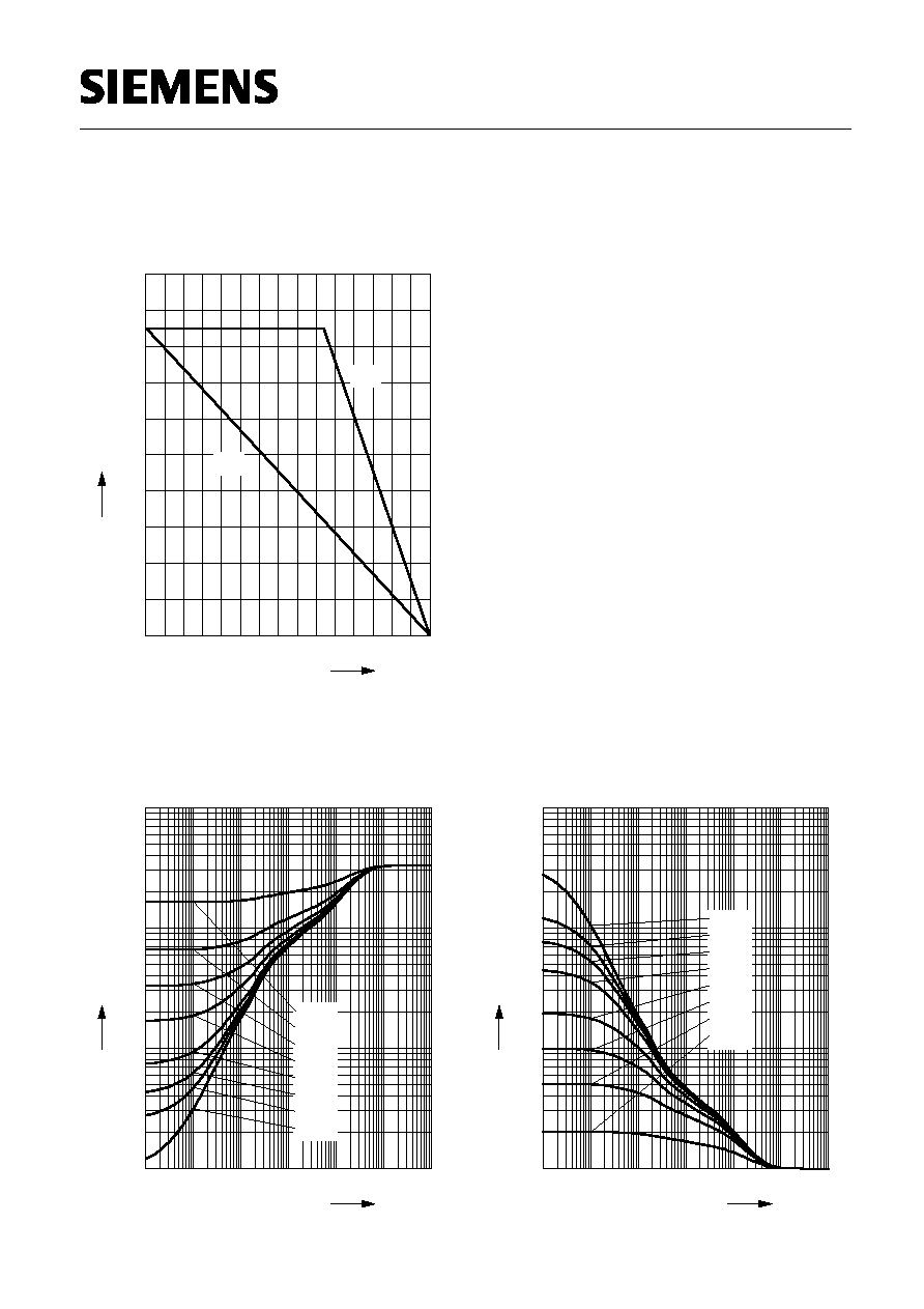
Total power dissipation
P
tot
=
f (T
A
*;
T
S
)
* Package mounted on epoxy
0
20
40
60
80
100
120 ∞C
150
T
A
,T
S
0
200
400
600
800
1000
1200
1400
1600
mW
2000
P
tot
T
S
T
A
Permissible Pulse Load
R
thJS
=
f (t
p
)
10
-6
10
-5
10
-4
10
-3
10
-2
10
0
s
t
p
-1
10
0
10
1
10
2
10
K/W
R
thJS
0.5
0.2
0.1
0.05
0.02
0.01
0.005
D = 0
Permissible Pulse Load
P
totmax
/
P
totDC
=
f (t
p
)
10
-6
10
-5
10
-4
10
-3
10
-2
10
0
s
t
p
0
10
1
10
2
10
3
10
-
P
totmax
/ P
totDC
D = 0
0.005
0.01
0.02
0.05
0.1
0.2
0.5
Semiconductor Group
3
1998-11-01
BCP 71M
Semiconductor Group
Au -12-1998
4
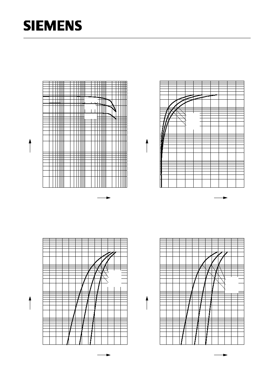
DC current gain
h
FE
=
f (I
C
)
V
CE
= 2V
10
0
10
1
10
2
10
3
10
4
mA
I
C
0
10
1
10
2
10
3
10
-
h
FE
-50∞C
25∞C
100∞C
Collector-emitter saturation voltage
I
C
=
f (V
CEsat
),
h
FE
= 10
0.00 0.05 0.10 0.15 0.20 0.25 0.30 0.35 0.40 V
0.50
V
CEsat
0
10
1
10
2
10
3
10
4
10
mA
I
C
100∞C
25∞C
-50∞C
Base-emitter saturation voltage
I
C
=
f (V
BEsat
),
h
FE
= 10
0.0
0.2
0.4
0.6
0.8
1.0
V
1.3
V
BEsat
0
10
1
10
2
10
3
10
4
10
mA
I
C
-50∞C
25∞C
100∞C
Collector current
I
C
=
f (V
BE
)
V
CE
= 2V
0.0
0.2
0.4
0.6
0.8
1.0
V
1.3
V
BE
0
10
1
10
2
10
3
10
4
10
mA
I
C
-50∞C
25∞C
100∞C
Semiconductor Group
4
1998-11-01