Semiconductor Group
1
NPN Silicon AF Transistors
BC 337
BC 338
5.91
Type
Marking
Package
1)
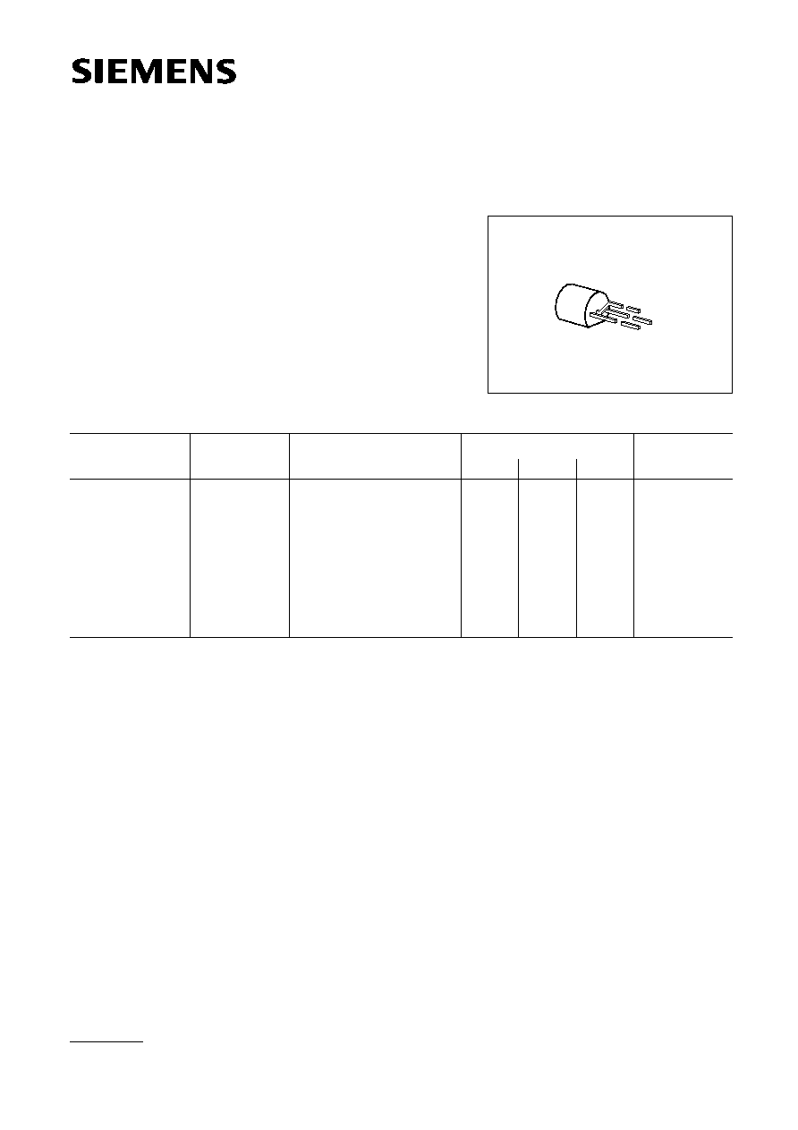
Pin Configuration
BC 337
BC 337-16
BC 337-25
BC 337-40
BC 338
BC 338-16
BC 338-25
BC 338-40
Q62702-C313
Q62702-C313-V3
Q62702-C313-V1
Q62702-C313-V2
Q62702-C314
Q62702-C314-V1
Q62702-C314-V2
Q62702-C314-V3
≠
TO-92
1
2
3
Ordering Code
C
B
E
1)
For detailed information see chapter Package Outlines.
q
High current gain
q
High collector current
q
Low collector-emitter saturation voltage
q
Complementary types: BC 327, BC 328 (PNP)
1
2
3
Semiconductor Group
2
BC 337
BC 338
Maximum Ratings
Parameter
Symbol
BC 337
Unit
Collector-emitter voltage
V
CE0
45
V
Collector-base voltage
V
CB0
50
Emitter-base voltage
V
EB0
Collector current
I
C
mA
Base current
I
B
mA
Total power dissipation,
T
C
= 66 ∞C
P
tot
mW
Junction temperature
T
j
∞C
Storage temperature range
T
stg
≠ 65 ... + 150
Thermal Resistance
Junction - ambient
R
th JA
200
K/W
Peak collector current
I
CM
A
Junction - case
1)
R
th JC
135
Peak base current
I
BM
BC 338
25
30
5
800
100
625
150
1
200
Values
1)
Mounted on Al heat sink 15 mm
◊
25 mm
◊
0.5 mm.
Semiconductor Group
3
BC 337
BC 338
Electrical Characteristics
at
T
A
= 25 ∞C, unless otherwise specified.
≠
DC current gain
1)
I
C
= 100 mA;
V
CE
= 1 V
BC 337/16; BC 338/16
BC 337/25; BC 338/25
BC 337/40; BC 338/40
I
C
= 300 mA;
V
CE
= 1 V
BC 337/16; BC 338/16
BC 337/25; BC 338/25
BC 337/40; BC 338/40
h
FE
100
160
250
60
100
170
160
250
350
≠
≠
≠
250
400
630
≠
≠
≠
V
Collector-emitter breakdown voltage
I
C
= 10 mA
BC 337
BC 338
V
(BR)CE0
45
25
≠
≠
≠
≠
nA
nA
µ
A
µ
A
Collector cutoff current
V
CB
= 25 V
BC 338
V
CB
= 45 V
BC 337
V
CB
= 25 V,
T
A
= 150 ∞C
BC 338
V
CB
= 45 V,
T
A
= 150 ∞C
BC 337
I
CB0
≠
≠
≠
≠
≠
≠
≠
≠
100
100
10
10
Unit
Values
Parameter
Symbol
min.
typ.
max.
DC characteristics
Collector-base breakdown voltage
I
C
= 100
µ
A
BC 337
BC 338
V
(BR)CB0
50
30
≠
≠
≠
≠
Emitter-base breakdown voltage
I
E
= 10
µ
A
V
(BR)EB0
5
≠
≠
V
Collector-emitter saturation voltage
1)
I
C
= 500 mA;
I
B
= 50 mA
V
CEsat
≠
≠
0.7
Base-emitter saturation voltage
I
C
= 500 mA;
I
B
= 50 mA
V
BEsat
≠
≠
2
nA
Emitter cutoff current
V
EB
= 4 V
I
EB0
≠
≠
100
1)
Pulse test:
t
300
µ
s,
D
2 %.

Semiconductor Group
4
BC 337
BC 338
Electrical Characteristics
at
T
A
= 25 ∞C, unless otherwise specified.
MHz
Transition frequency
I
C
= 50 mA,
V
CE
= 5 V,
f
= 20 MHz
f
T
≠
170
≠
Unit
Values
Parameter
Symbol
min.
typ.
max.
AC characteristics
pF
Output capacitance
V
CB
= 10 V,
f
= 1 MHz
C
obo
≠
8
≠
Input capacitance
V
EB
= 0.5 V,
f
= 1 MHz
C
ibo
≠
60
≠
Semiconductor Group
5
BC 337
BC 338
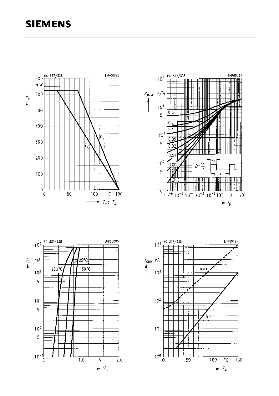
Total power dissipation
P
tot
=
f
(
T
A
;
T
C
)
Collector current
I
C
=
f
(
V
BE
)
V
CE
= 1 V
Permissible pulse load
R
thJA
=
f
(
t
p
)
Collector cutoff current
I
CB0
=
f
(
T
A
)
V
CB
= 45 V
Semiconductor Group
6
BC 337
BC 338
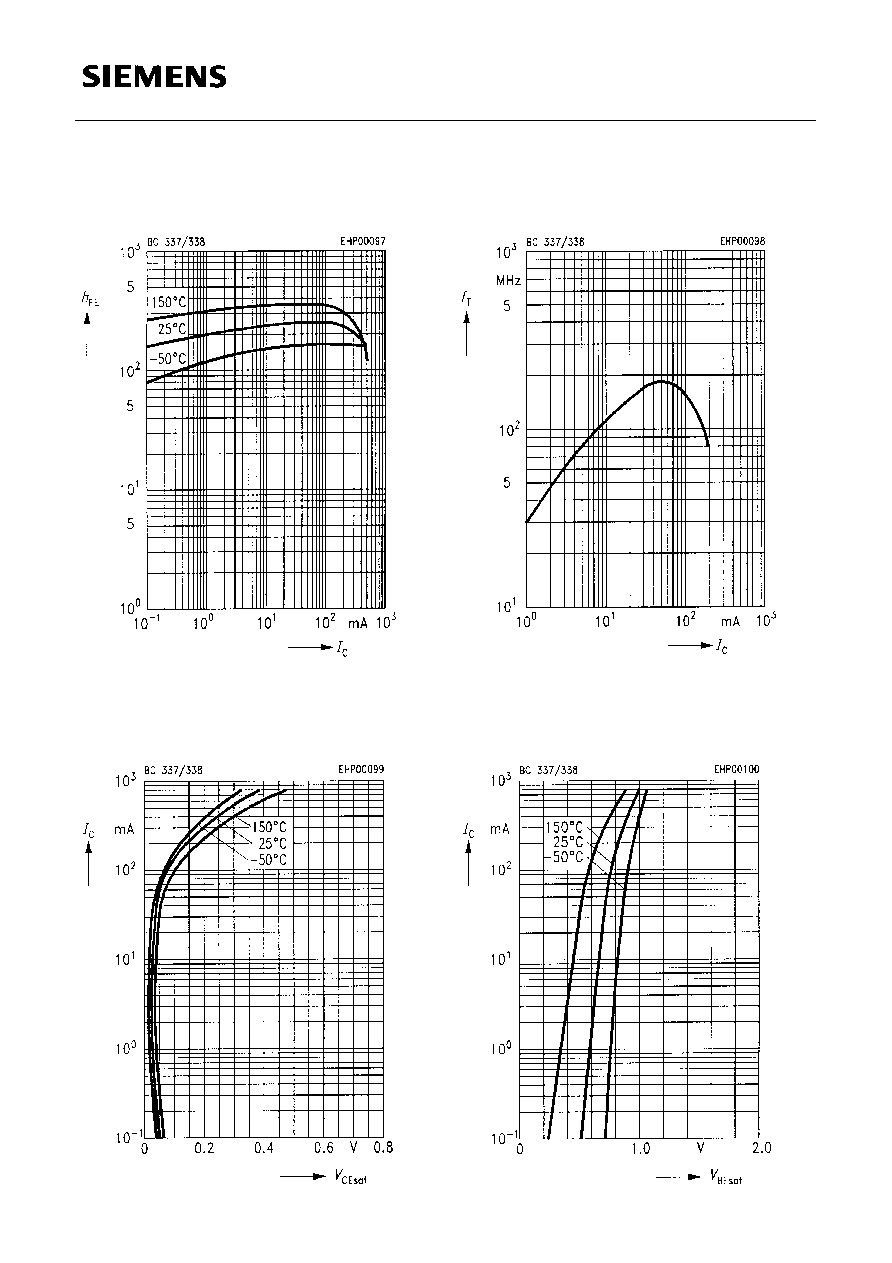
Transition frequency
f
T
=
f
(
I
C
)
f
= 20 MHz,
T
A
= 25 ∞C
Base-emitter saturation voltage
V
BEsat
=
f
(
I
C
)
h
FE
= 10
DC current gain
h
FE
=
f
(
I
C
)
V
CE
= 1 V
Collector-emitter saturation voltage
V
CEsat
=
f
(
I
C
)
h
FE
= 10