Semiconductor Group
1
04.96
Silicon N Channel MOSFET Tetrode
BF 998
Features
q
Short-channel transistor
with high S/C quality factor
q
For low-noise, gain-controlled
input stages up to 1 GHz
Maximum Ratings
Type
Marking
Package
1)
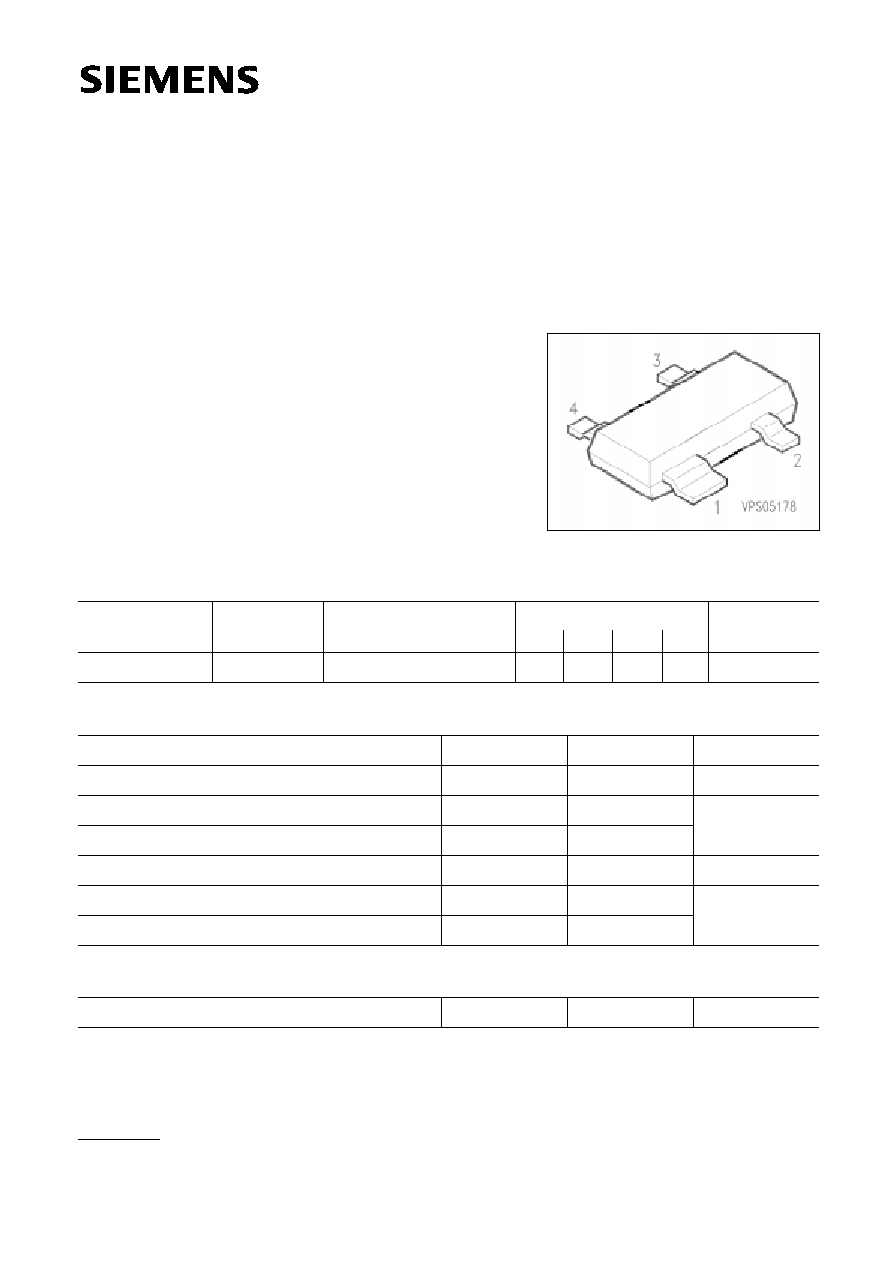
Pin Configuration
BF 998
Q62702-F1129
MO
SOT-143
1
2
3
4
S
D
G
2
G
1
Ordering Code
(tape and reel)
Parameter
Symbol
Values
Unit
Drain-source voltage
V
DS
12
V
Thermal Resistance
Junction - soldering point
R
th JS
< 370
K/W
Total power dissipation,
T
S
< 76 �C
P
tot
200
mW
Storage temperature range
T
stg
� 55 ... + 150
�C
Gate 1/gate 2 peak source current
�
I
G1/2SM
10
Channel temperature
T
ch
150
mA
Drain current
I
D
30
1)
For detailed information see chapter Package Outlines.
BF 998
Semiconductor Group
2
Electrical Characteristics
at
T
A
= 25 �C, unless otherwise specified.
Unit
Values
Parameter
Symbol
min.
typ.
max.
V
Drain-source breakdown voltage
I
D
= 10
�
A,
� V
G1S
= �
V
G2S
= 4 V
V
(BR) DS
12
�
�
nA
Gate 1-source leakage current
�
V
G1S
= 5 V,
V
G2S
=
V
DS
= 0
�
I
G1SS
�
�
50
Gate 1-source breakdown voltage
�
I
G1S
= 10 mA,
V
G2S
=
V
DS
= 0
�
V
(BR) G1SS
8
�
12
Gate 2-source breakdown voltage
�
I
G2S
= 10 mA,
V
G1S
=
V
DS
= 0
�
V
(BR) G2SS
8
�
12
Gate 2-source leakage current
�
V
G2S
= 5 V,
V
G1S
=
V
DS
= 0
�
I
G2SS
�
�
50
mA
Drain current
V
DS
= 8 V,
V
G1S
= 0
, V
G2S
= 4 V
I
DSS
2
�
18
V
Gate 1-source pinch-off voltage
V
DS
= 8 V,
V
G2S
= 4 V
, I
D
= 20
�
A
� V
G1S(p)
�
�
2.5
Gate 2-source pinch-off voltage
V
DS
= 8 V,
V
G1S
= 0
, I
D
= 20
�
A
� V
G2S(p)
�
�
2
DC Characteristics

BF 998
Semiconductor Group
3
Electrical Characteristics
at
T
A
= 25 �C, unless otherwise specified.
Control range
(test circuit 2)
V
DS
= 8 V,
V
G2S
= 4 ... � 2 V
f
= 800 MHz
G
ps
40
�
�
dB
Noise figure
(test circuit 1)
V
DS
= 8 V,
I
D
= 10 mA,
f
= 200 MHz,
G
G
= 2 mS,
G
L
= 0.5 mS,
V
G2S
= 4 V
F
�
0.6
�
Noise figure
(test circuit 2)
V
DS
= 8 V,
I
D
= 10 mA,
f
= 800 MHz,
G
G
= 3.3 mS,
G
L
= 1 mS,
V
G2S
= 4 V
F
�
1
�
Unit
Values
mS
Parameter
Forward transconductance
V
DS
= 8 V,
I
D
= 10 mA,
V
G2S
= 4 V
f
= 1 kHz
Symbol
g
fs
min.
�
typ.
24
max.
�
pF
Gate 1 input capacitance
V
DS
= 8 V,
I
D
= 10 mA,
V
G2S
= 4 V
f
= 1 MHz
C
g1ss
�
2.1
2.5
Gate 2 input capacitance
V
DS
= 8 V,
I
D
= 10 mA,
V
G2S
= 4 V
f
= 1 MHz
C
g2ss
�
1.2
�
fF
Reverse transfer capacitance
V
DS
= 8 V,
I
D
= 10 mA,
V
G2S
= 4 V
f
= 1 MHz
C
dg1
�
25
�
pF
Output capacitance
V
DS
= 8 V,
I
D
= 10 mA,
V
G2S
= 4 V
f
= 1 MHz
C
dss
�
1.05
�
dB
Power gain
(test circuit 1)
V
DS
= 8 V,
I
D
= 10 mA,
f
= 200 MHz,
G
G
= 2 mS,
G
L
= 0.5 mS,
V
G2S
= 4 V
G
ps
�
28
�
Power gain
(test circuit 2)
V
DS
= 8 V,
I
D
= 10 mA,
f
= 800 MHz,
G
G
= 3.3 mS,
G
L
= 1 mS,
V
G2S
= 4 V
G
ps
�
20
�
AC Characteristics
BF 998
Semiconductor Group
4
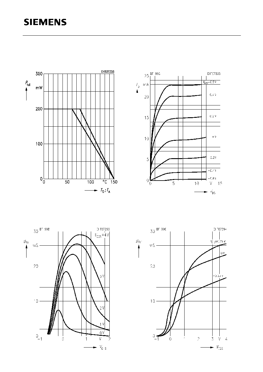
Total power dissipation
P
tot
=
f
(
T
A
)
Gate 1 forward transconductance
g
fs1
=
f
(
V
G1S
)
V
DS
= 8 V,
I
DSS
= 10 mA,
f
= 1 kHz
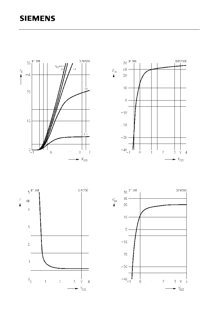
Output characteristics
I
D
=
f
(
V
DS
)
V
G2S
= 4 V
Gate 1 forward transconductance
g
fs1
=
f
(
V
G2S
)
V
DS
= 8 V,
I
DSS
= 10 mA,
f
= 1 kHz
BF 998
Semiconductor Group
5
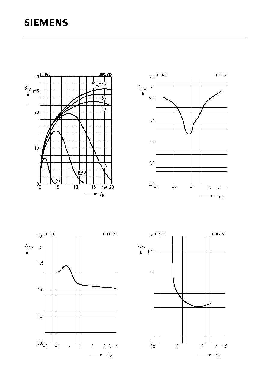
Gate 1 forward transconductance
g
fs1
=
f
(
I
D
)
V
DS
= 8 V,
I
DSS
= 10 mA,
f
= 1 kHz
Gate 2 input capacitance
C
g2ss
=
f
(
V
G2S
)
V
G1S
= 0 V,
V
DS
= 8 V
I
DSS
= 10 mA,
f
= 1 MHz
Gate 1 input capacitance
C
g1ss
=
f
(
V
G1S
)
V
G2S
= 4 V,
V
DS
= 8 V,
I
DSS
= 10 mA,
f
= 1 MHz
Output capacitance
C
dss
=
f
(
V
DS
)
V
G1S
= 0 V,
V
G2S
= 4 V
I
DSS
= 10 mA,
f
= 1 MHz
BF 998
Semiconductor Group
6
Drain current
I
D
=
f
(
V
G1S
)
V
DS
= 8 V
Noise figure
F
=
f
(
V
G2S
)
V
DS
= 8 V,
V
G1S
= 0,
I
DSS
= 10 mA,
f
= 200 MHz (see test circuit 1)
Power gain
G
ps
=
f
(
V
G2S
)
V
DS
= 8 V,
V
G1S
= 0,
I
DSS
= 10 mA,
f
= 200 MHz (see test circuit 1)
Power gain
G
ps
=
f
(
V
G2S
)
V
DS
= 8 V,
V
G1S
= 0,
I
DSS
= 10 mA,
f
= 800 MHz (see test circuit 2)
BF 998
Semiconductor Group
7
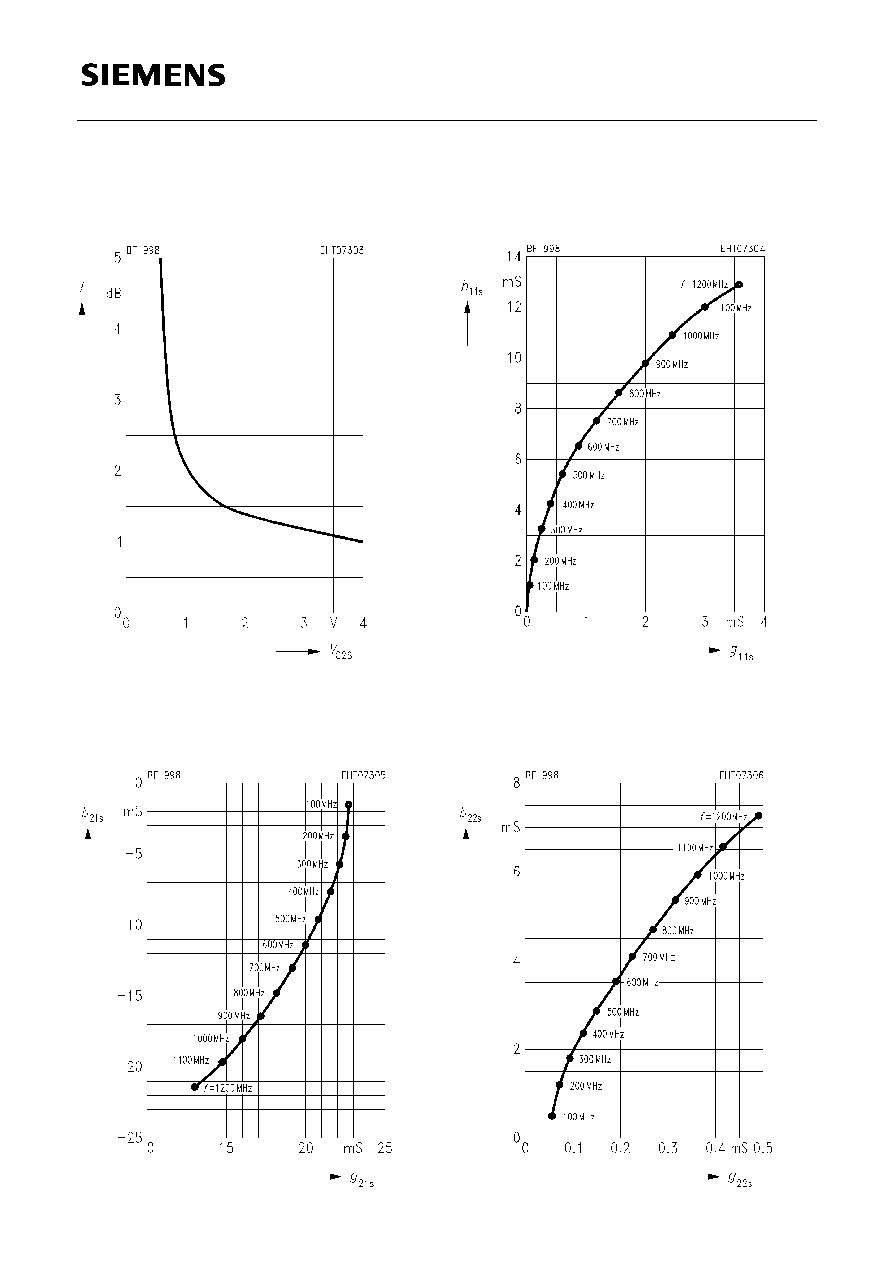
Noise figure
F
=
f
(
V
G2S
)
V
DS
= 8 V,
V
G1S
= 0,
I
DSS
= 10 mA,
f
= 800 MHz (see test circuit 2)
Gate 1 forward transfer admittance
y
21s
V
DS
= 8 V,
V
G2S
= 4 V,
V
G1S
= 0
I
DSS
= 10 mA (common-source)
Gate 1 input admittance
y
11s
V
DS
= 8 V,
V
G2S
= 4 V,
V
G1S
= 0,
I
DSS
= 10 mA (common-source)
Output admittance
y
22s
V
DS
= 8 V,
V
G2S
= 4 V,
V
G1S
= 0
I
DSS
= 10 mA (common-source)

BF 998
Semiconductor Group
8
Test circuit 1 for power gain and noise figure
f
= 200 MHz,
G
G
= 2 mS,
G
L
= 0.5 mS
Test circuit 2 for power gain and noise figure
f
= 800 MHz,
G
G
= 3.3 mS,
G
L
= 1 mS