
Semiconductor Group
1
04.96
GaAs FET
CF 739
Features
q
N-channel dual-gate GaAs MES FET
q
Depletion mode transistor for tuned small-signal
applications up to 2 GHz, e. g. VHF, UHF,
Sat-TV tuners
q
Low noise
q
High gain
q
Low input capacitance
ESD: Electrostatic discharge sensitive device, observe handling precautions!
Maximum Ratings
1
2
3
S
D
G
2
4
G
1
Type
Ordering Code
(tape and reel)
Marking
Package
1)
Pin Configuration
CF 739
Q62702-F1215
MS
SOT-143
Parameter
Symbol
Values
Unit
Drain-source voltage
V
DS
10
V
Drain current
I
D
80
mA
Gate 2-source voltage
≠
V
G2S
6
Channel temperature
T
ch
150
∞C
Total power dissipation,
T
S
66 ∞C
2)
P
tot
240
mW
Storage temperature range
T
stg
≠ 55 ... + 150
Thermal Resistance
Channel - soldering point
3)
R
thchS
350
K/W
Gate 1-source voltage
≠
V
G1S
6
Gate 1-source peak current
+
I
G1SM
1
Gate 2-source peak current
+
I
G2SM
1
1)
For detailed information see chapter Package Outlines.
2)
Package mounted on alumina 15 mm
◊
16.7 mm
◊
0.7 mm.
3)
T
S
is measured on the source lead at the soldering point to the pcb.
CF 739
Semiconductor Group
2
Electrical Characteristics
at
T
A
= 25 ∞C, unless otherwise specified.
V
Drain-source breakdown voltage
I
D
= 100
µ
A, ≠
V
G1S
= ≠
V
G2S
= 4 V
V
(BR)DS
10
≠
≠
V
Gate 1-source pinch-off voltage
V
G2S
= 0,
V
DS
= 5 V,
I
D
= 200
µ
A
≠
V
G1S(P)
≠
≠
2.5
Gate 2-source pinch-off voltage
V
G1S
= 0,
V
DS
= 5 V,
I
D
= 200
µ
A
≠
V
G2S(P)
≠
≠
2.5
mA
Drain current
V
G1S
= 0,
V
G2S
= 0,
V
DS
= 3 V
I
DSS
6
≠
60
Unit
Values
Parameter
Symbol
min.
typ.
max.
DC Characteristics
µ
A
Gate 1 leakage current
≠
V
G1S
= 5 V
, V
G2S
=
V
DS
= 0
≠
I
G1SS
≠
≠
20
Gate 2 leakage current
≠
V
G2S
= 5 V
, V
G1S
=
V
DS
= 0
≠
I
G2SS
≠
≠
20
AC Characteristics
mS
Forward transconductance
V
DS
= 5 V,
V
G2S
= 2 V,
I
D
= 10 mA,
f
= 1 kHz
g
fs
≠
25
≠
Output capacitance
V
G2S
= 2 V,
V
DS
= 5 V,
I
D
= 10 mA,
f
= 1 MHz
C
dss
≠
0.5
≠
dB
Noise figure
V
G2S
= 2 V,
V
DS
= 5 V,
I
D
= 10 mA,
f
= 1.75 GHz
V
G2S
= 2 V,
V
DS
= 5 V,
I
D
= 10 mA,
f
= 800 MHz
F
≠
≠
1.8
1.1
≠
≠
pF
Gate 1 input capacitance
V
G2S
= 2 V,
V
DS
= 5 V,
I
D
= 10 mA,
f
= 1 MHz
C
gfss
≠
0.95
≠
Control range
V
G2S
= 2 V ... ≠ 3 V
G
psc
≠
50
≠
Power gain
V
G2S
= 2 V,
V
DS
= 5 V,
I
D
= 10 mA,
f
= 1.75 GHz
V
G2S
= 2 V,
V
DS
= 5 V,
I
D
= 10 mA,
f
= 800 MHz
G
ps
≠
≠
17
22
≠
≠
CF 739
Semiconductor Group
3
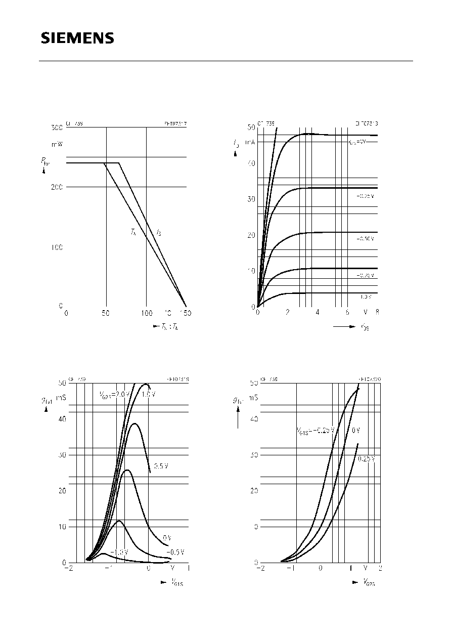
Total power dissipation
P
tot
=
f
(
T
A
*;
T
S
)
*Package mounted on alumina
Gate 1 forward transconductance
g
fs1
=
f
(
V
G1S
)
V
DS
= 5 V,
f
= 1 kHz
Output characteristics
I
D
=
f
(
V
DS
)
V
G2S
= 2 V
Gate 1 forward transconductance
g
fs1
=
f
(
V
G2S
)
V
DS
= 5 V,
f
= 1 kHz

CF 739
Semiconductor Group
5
Gate 1 input admittance
y
11s
V
DS
= 5 V,
V
G2S
= 2 V,
I
D
= 10 mA
Output admittance
y
22s
V
DS
= 5 V,
V
G2S
= 2 V,
I
D
= 10 mA
Gate 1 forward transfer admittance
y
21s
V
DS
= 5 V,
V
G2S
= 2 V,
I
D
= 10 mA
Common Source Admittance Parameters,
G
2
RF grounded
