Semiconductor Group
1
Dec-11-1996
BFR 106
NPN Silicon RF Transistor
∑ For low noise, high-gain amplifiers
∑ For linear broadband amplifiers
∑ Special application: antenna amplifiers
∑ Complementary type: BFR 194 (PNP)
ESD: Electrostatic discharge sensitive device, observe handling precaution!
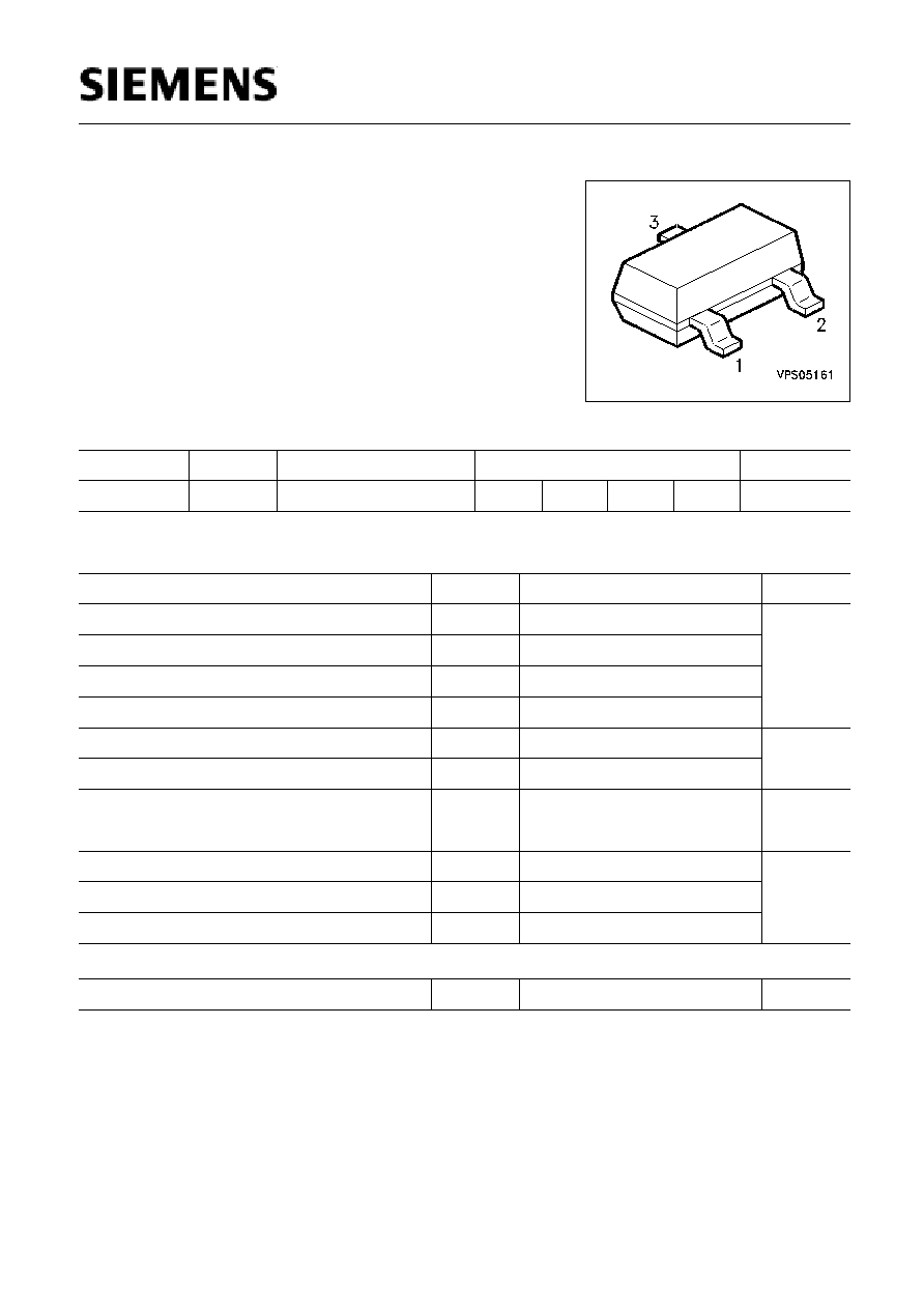
Type
Marking Ordering Code
Pin Configuration
Package
BFR 106
R7s
Q62702-F1219
1 = B
2 = E
3 = C 4 = E
SOT-23
Maximum Ratings
Parameter
Symbol
Values
Unit
Collector-emitter voltage
V
CEO
15
V
Collector-emitter voltage
V
CES
20
Collector-base voltage
V
CBO
20
Emitter-base voltage
V
EBO
3
Collector current
I
C
100
mA
Base current
I
B
12
Total power dissipation
T
S
73 ∞C
P
tot
700
mW
Junction temperature
T
j
150
∞C
Ambient temperature
T
A
- 65 ... + 150
Storage temperature
T
stg
- 65 ... + 150
Thermal Resistance
Junction - soldering point
1)
R
thJS
110
K/W
1)
T
S
is measured on the collector lead at the soldering point to the pcb.

Semiconductor Group
2
Dec-11-1996
BFR 106
Electrical Characteristics at
T
A
= 25∞C, unless otherwise specified.
Parameter
Symbol
Values
Unit
min.
typ.
max.
DC Characteristics
Collector-emitter breakdown voltage
I
C
= 1 mA,
I
B
= 0
V
(BR)CEO
15
-
-
V
Collector-emitter cutoff current
V
CE
= 20 V,
V
BE
= 0
I
CES
-
-
100
µA
Collector-base cutoff current
V
CB
= 10 V,
I
E
= 0
I
CBO
-
-
100
nA
Emitter-base cutoff current
V
EB
= 2 V,
I
C
= 0
I
EBO
-
-
10
µA
DC current gain
I
C
= 70 mA,
V
CE
= 8 V
h
FE
40
100
220
-

Semiconductor Group
3
Dec-11-1996
BFR 106
Electrical Characteristics at
T
A
= 25∞C, unless otherwise specified.
Parameter
Symbol
Values
Unit
min.
typ.
max.
AC Characteristics
Transition frequency
I
C
= 70 mA,
V
CE
= 8 V,
f = 500 MHz
f
T
3.5
5
-
GHz
Collector-base capacitance
V
CB
= 10 V,
f = 1 MHz
C
cb
-
0.95
1.5
pF
Collector-emitter capacitance
V
CE
= 10 V,
f = 1 MHz
C
ce
-
0.25
-
Emitter-base capacitance
V
EB
= 0.5 V,
f = 1 MHz
C
eb
-
4.4
-
Noise figure
I
C
= 20 mA,
V
CE
= 8 V,
Z
S
=
Z
Sopt
f = 900 MHz
f = 1.8 GHz
F
-
-
4
2.5
-
-
dB
Power gain
2)
I
C
= 70 mA,
V
CE
= 8 V,
Z
S
=
Z
Sopt
Z
L
=
Z
Lopt
f = 900 MHz
f = 1.8 GHz
G
ma
-
-
7.5
12.5
-
-
Transducer gain
I
C
= 70 mA,
V
CE
= 8 V,
Z
S
=
Z
L
= 50
f = 900 MHz
f = 1.8 GHz
|
S
21e
|
2
-
-
5
10.5
-
-
2)
G
ma
= |
S
21
/
S
12
| (k-(k
2
-1)
1/2
)
Semiconductor Group
4
Dec-11-1996
BFR 106
SPICE Parameters (Gummel-Poon Model, Berkeley-SPICE 2G.6 Syntax) :
Transistor Chip Data
IS =
1.8998
fA
VAF =
15
V
NE =
1.3235
-
VAR =
4.1613
V
NC =
1.4602
-
RBM =
1.0893
CJE =
5.0933
fF
TF =
35.78
ps
ITF =
62.059
mA
VJC =
0.81533
V
TR =
1.2466
ns
MJS =
0
-
XTI =
3
-
BF =
132.75
-
IKF =
0.44125
A
BR =
11.407
-
IKR =
0.010016
A
RB =
1.2652
RE =
1.1351
VJE =
0.85909
V
XTF =
0.44444
-
PTF =
0
deg
MJC =
0.46849
-
CJS =
0
fF
XTB =
0
-
FC =
0.92887
-
NF =
0.89608
-
ISE =
71.424
fA
NR =
0.91008
-
ISC =
2.0992
fA
IRB =
0.028135
mA
RC =
0.27485
MJE =
0.69062
-
VTF =
0.10681
V
CJC =
2327.8
fF
XCJC =
0.14496
-
VJS =
0.75
V
EG =
1.11
eV
TNOM
300
K
All parameters are ready to use, no scalling is necessary.
Extracted on behalf of SIEMENS Small Signal Semiconductors by:
Institut f¸r Mobil-und Satellitenfunktechnik (IMST)
© 1996 SIEMENS AG
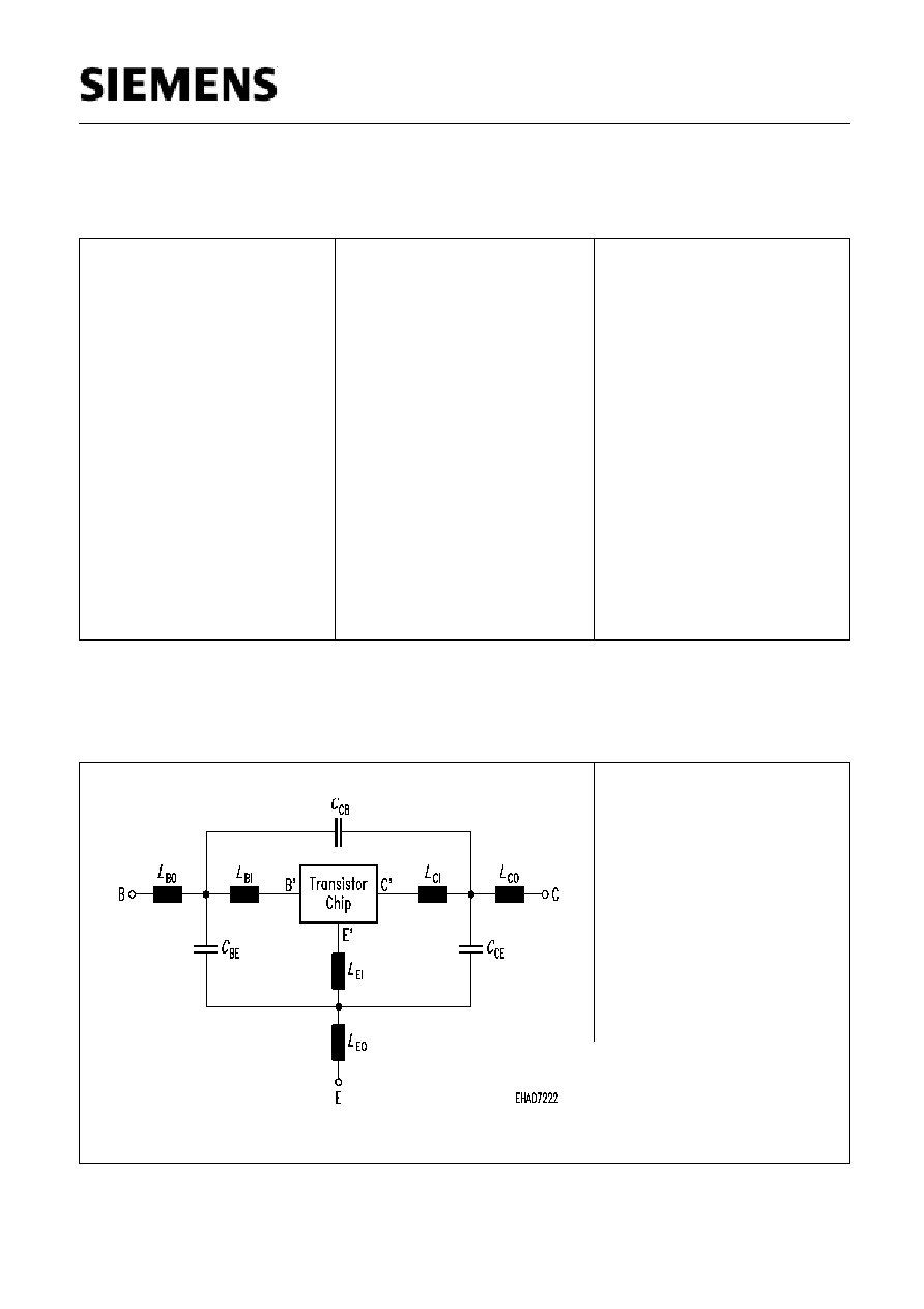
Package Equivalent Circuit:
LBI =
0.85
nH
LBO =
0.51
nH
LEI =
0.69
nH
LEO =
0.61
nH
LCI =
0
nH
LCO =
0.43
nH
CBE =
73
fF
CCB =
84
fF
CCE =
165
fF
Valid up to 6 GHz
For examples and ready to use parameters please contact your local Siemens distributor or sales office to
obtain a Siemens CD-ROM or see Internet: http://www.siemens.de/Semiconductor/products/35/35.htm
Semiconductor Group
5
Dec-11-1996
BFR 106
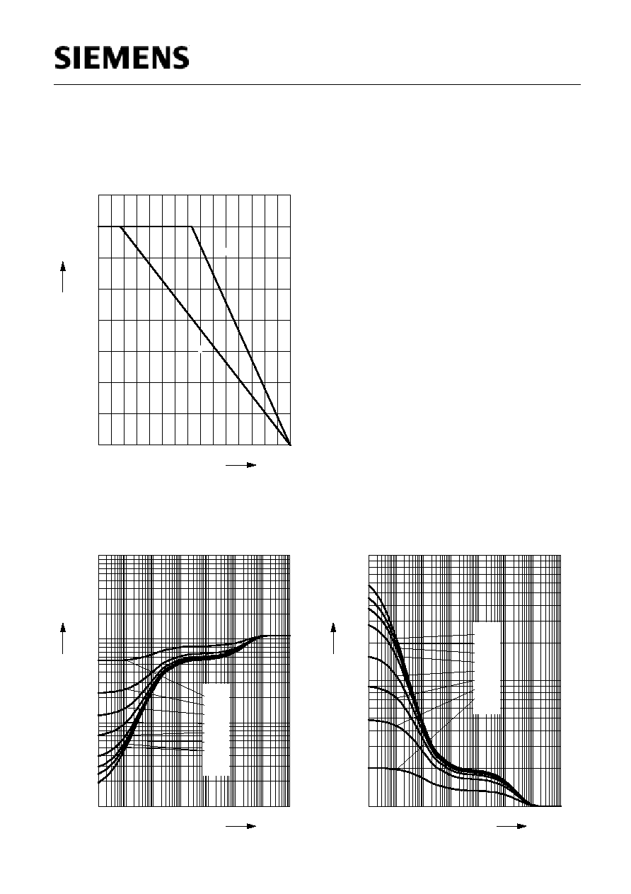
Total power dissipation
P
tot
=
f (T
A
*,
T
S
)
* Package mounted on epoxy
0
20
40
60
80
100
120 ∞C 150
T
A
,T
S
0
100
200
300
400
500
600
mW
800
P
tot
T
S
T
A
Permissible Pulse Load
R
thJS
=
f (t
p
)
10
-7
10
-6
10
-5
10
-4
10
-3
10
-2
10
-1
10
0
s
t
p
0
10
1
10
2
10
3
10
K/W
R
thJS
D = 0
0.005
0.01
0.02
0.05
0.1
0.2
0.5
Permissible Pulse Load
P
totmax
/
P
totDC
=
f (t
p
)
10
-7
10
-6
10
-5
10
-4
10
-3
10
-2
10
-1
10
0
s
t
p
0
10
1
10
2
10
-
P
totmax
/
P
totDC
D = 0
0.005
0.01
0.02
0.05
0.1
0.2
0.5
Semiconductor Group
6
Dec-11-1996
BFR 106
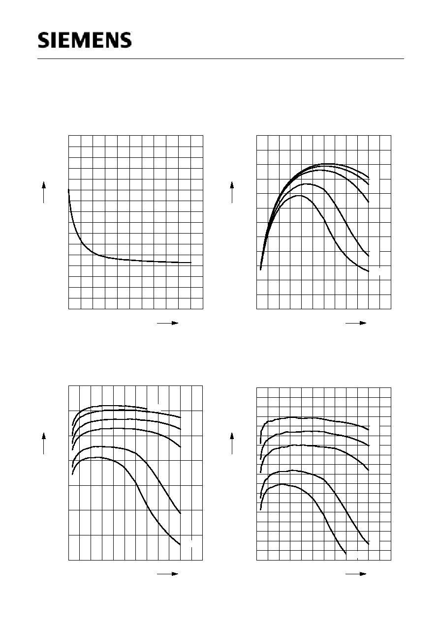
Collector-base capacitance
C
cb
=
f (V
CB
)
V
BE
=
v
be
= 0,
f = 1MHz
0
4
8
12
16
V
22
V
R
0.0
0.4
0.8
1.2
1.6
2.0
2.4
pF
3.2
C
cb
Transition frequency
f
T
=
f (I
C
)
V
CE
= Parameter
0
20
40
60
80
mA
120
I
C
0.0
0.5
1.0
1.5
2.0
2.5
3.0
3.5
4.0
4.5
5.0
GHz
6.0
f
T
5V
3V
2V
1V
0.7V
Power Gain
G
ma
,
G
ms
=
f(I
C
)
f = 0.9GHz
V
CE
= Parameter
0
20
40
60
80
mA
120
I
C
0
2
4
6
8
10
dB
14
G
10V
5V
3V
2V
1V
0.7V
Power Gain
G
ma
,
G
ms
=
f(I
C
)
f = 1.8GHz
V
CE
= Parameter
0
20
40
60
80
mA
120
I
C
0.0
1.0
2.0
3.0
4.0
5.0
6.0
7.0
dB
9.0
G
5V
3V
2V
1V
0.7V

Semiconductor Group
7
Dec-11-1996
BFR 106
Power Gain
G
ma
,
G
ms
=
f(V
CE
):_____
|
S
21
|
2
=
f(V
CE
):---------
f = Parameter
0
2
4
6
8
V
12
V
CE
0
2
4
6
8
10
dB
14
G
0.9GHz
1.8GHz
0.9GHz
1.8GHz
I
C
=70mA
Intermodulation Intercept Point
IP
3
=
f(I
C
)
(3rd order, Output,
Z
S
=
Z
L
=50
)
V
CE
= Parameter,
f = 900MHz
0
10
20
30
40
50
60
70
80
mA 100
I
C
14
16
18
20
22
24
26
28
30
32
dBm
36
IP
3
8V
5V
3V
2V
1V
Power Gain
G
ma
,
G
ms
=
f(f)
V
CE
= Parameter
0.0
0.5
1.0
1.5
2.0
2.5
3.0
GHz
4.0
f
-5
0
5
10
15
20
25
30
35
dB
45
G
10V
1V
0.7V
I
C
=70mA
Power Gain |
S
21
|
2
=
f(f)
V
CE
= Parameter
0.0
0.5
1.0
1.5
2.0
2.5
GHz
3.5
f
-5
0
5
10
15
20
25
30
dB
40
S
21
10V
1V
0.7V
I
C
=70mA