Semiconductor Group
1
Dec-13-1996
BFG 196
NPN Silicon RF Transistor
∑ For low noise, low distortion broadband
amplifiers in antenna and telecommunications
systems up to 1.5GHz at collector currents from
20mA to 80mA
∑ Power amplifier for DECT and PCN systems
∑
f
T
= 7.5GHz
F = 1.5 dB at 900MHz
ESD: Electrostatic discharge sensitive device, observe handling precaution!
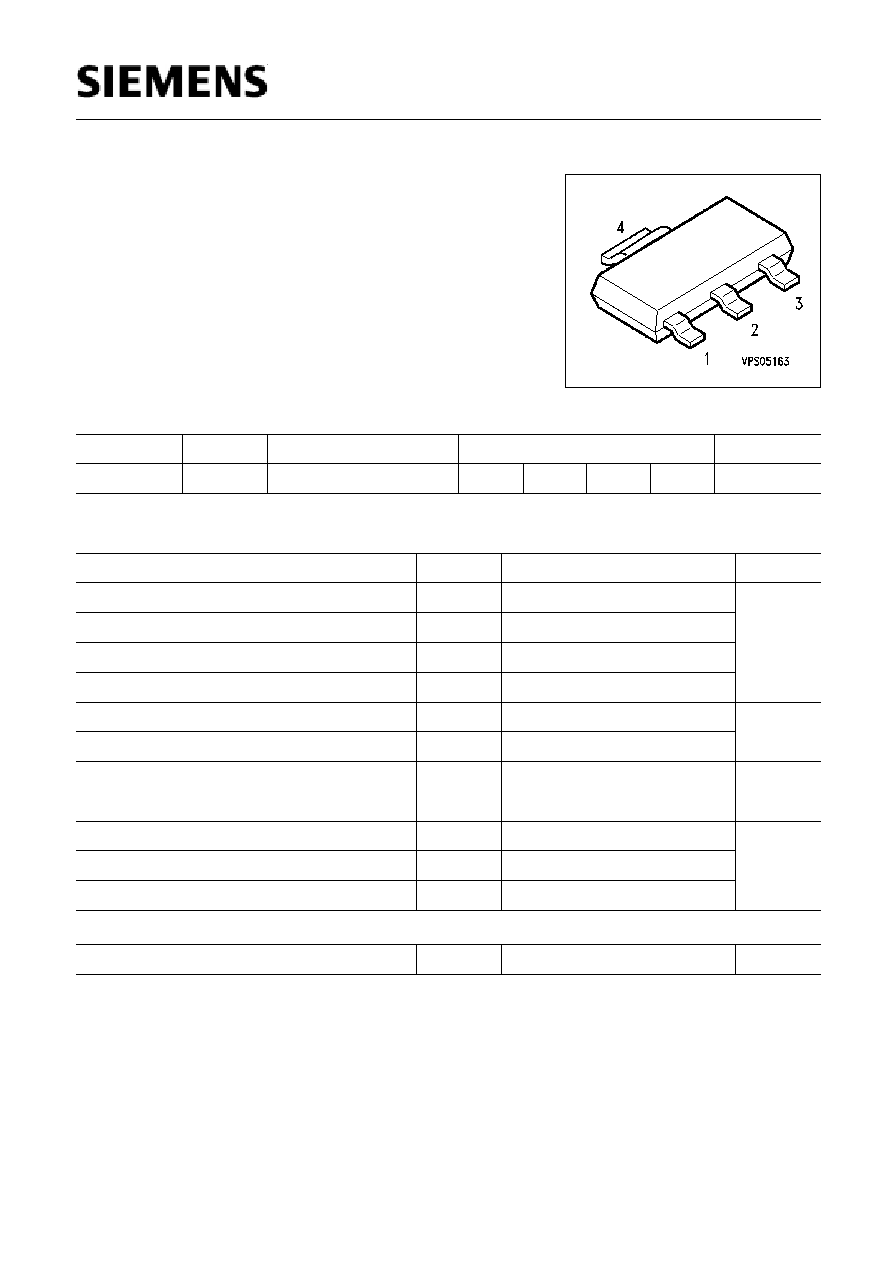
Type
Marking Ordering Code
Pin Configuration
Package
BFG 196
BFG196
Q62702-F1292
1 = E
2 = B
3 = E 4 = C
SOT-223
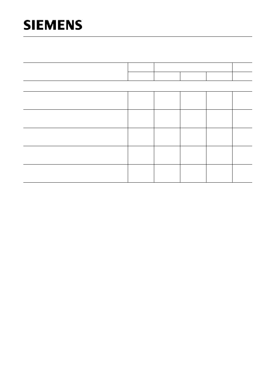
Maximum Ratings
Parameter
Symbol
Values
Unit
Collector-emitter voltage
V
CEO
12
V
Collector-emitter voltage
V
CES
20
Collector-base voltage
V
CBO
20
Emitter-base voltage
V
EBO
2
Collector current
I
C
100
mA
Base current
I
B
12
Total power dissipation
T
S
90 ∞C
P
tot
800
mW
Junction temperature
T
j
150
∞C
Ambient temperature
T
A
- 65 ... + 150
Storage temperature
T
stg
- 65 ... + 150
Thermal Resistance
Junction - soldering point
1)
R
thJS
75
K/W
1)
T
S
is measured on the collector lead at the soldering point to the pcb.
Semiconductor Group
2
Dec-13-1996
BFG 196
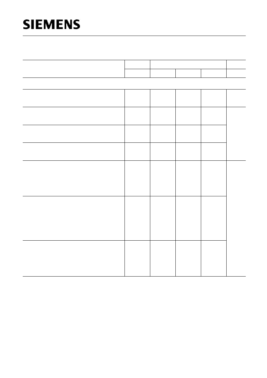
Electrical Characteristics at
T
A
= 25∞C, unless otherwise specified.
Parameter
Symbol
Values
Unit
min.
typ.
max.
DC Characteristics
Collector-emitter breakdown voltage
I
C
= 1 mA,
I
B
= 0
V
(BR)CEO
12
-
-
V
Collector-emitter cutoff current
V
CE
= 20 V,
V
BE
= 0
I
CES
-
-
100
µA
Collector-base cutoff current
V
CB
= 10 V,
I
E
= 0
I
CBO
-
-
100
nA
Emitter-base cutoff current
V
EB
= 1 V,
I
C
= 0
I
EBO
-
-
1
µA
DC current gain
I
C
= 50 mA,
V
CE
= 8 V
h
FE
50
100
200
-
Semiconductor Group
3
Dec-13-1996
BFG 196
Electrical Characteristics at
T
A
= 25∞C, unless otherwise specified.
Parameter
Symbol
Values
Unit
min.
typ.
max.
AC Characteristics
Transition frequency
I
C
= 70 mA,
V
CE
= 8 V,
f = 500 MHz
f
T
5
7.5
-
GHz
Collector-base capacitance
V
CB
= 10 V,
f = 1 MHz
C
cb
-
0.97
1.4
pF
Collector-emitter capacitance
V
CE
= 10 V,
f = 1 MHz
C
ce
-
0.4
-
Emitter-base capacitance
V
EB
= 0.5 V,
f = 1 MHz
C
eb
-
4
-
Noise figure
I
C
= 20 mA,
V
CE
= 8 V,
Z
S
=
Z
Sopt
f = 900 MHz
f = 1.8 GHz
F
-
-
2.5
1.5
-
-
dB
Power gain
2)
I
C
= 50 mA,
V
CE
= 8 V,
Z
S
=
Z
Sopt
Z
L
=
Z
Lopt
f = 900 MHz
f = 1.8 GHz
G
ma
-
-
8.5
14
-
-
Transducer gain
I
C
= 50 mA,
V
CE
= 8 V,
Z
S
=
Z
L
= 50
f = 900 MHz
f = 1.8 GHz
|
S
21e
|
2
-
-
6
11.5
-
-
2)
G
ma
= |
S
21
/
S
12
| (k-(k
2
-1)
1/2
)