Semiconductor Group
1
Silicon N Channel MOS FET Triode
BF 543
Preliminary Data
q
For RF stages up to 300 MHz
preferably in FM applications
q
I
DSS
= 4 mA,
g
fs
= 12 mS
ESD: Electrostatic discharge sensitive device, observe handling precautions!
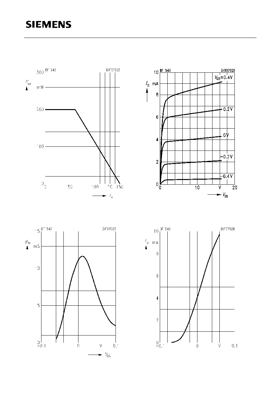
Maximum Ratings
Type
Ordering Code
(tape and reel)
Marking
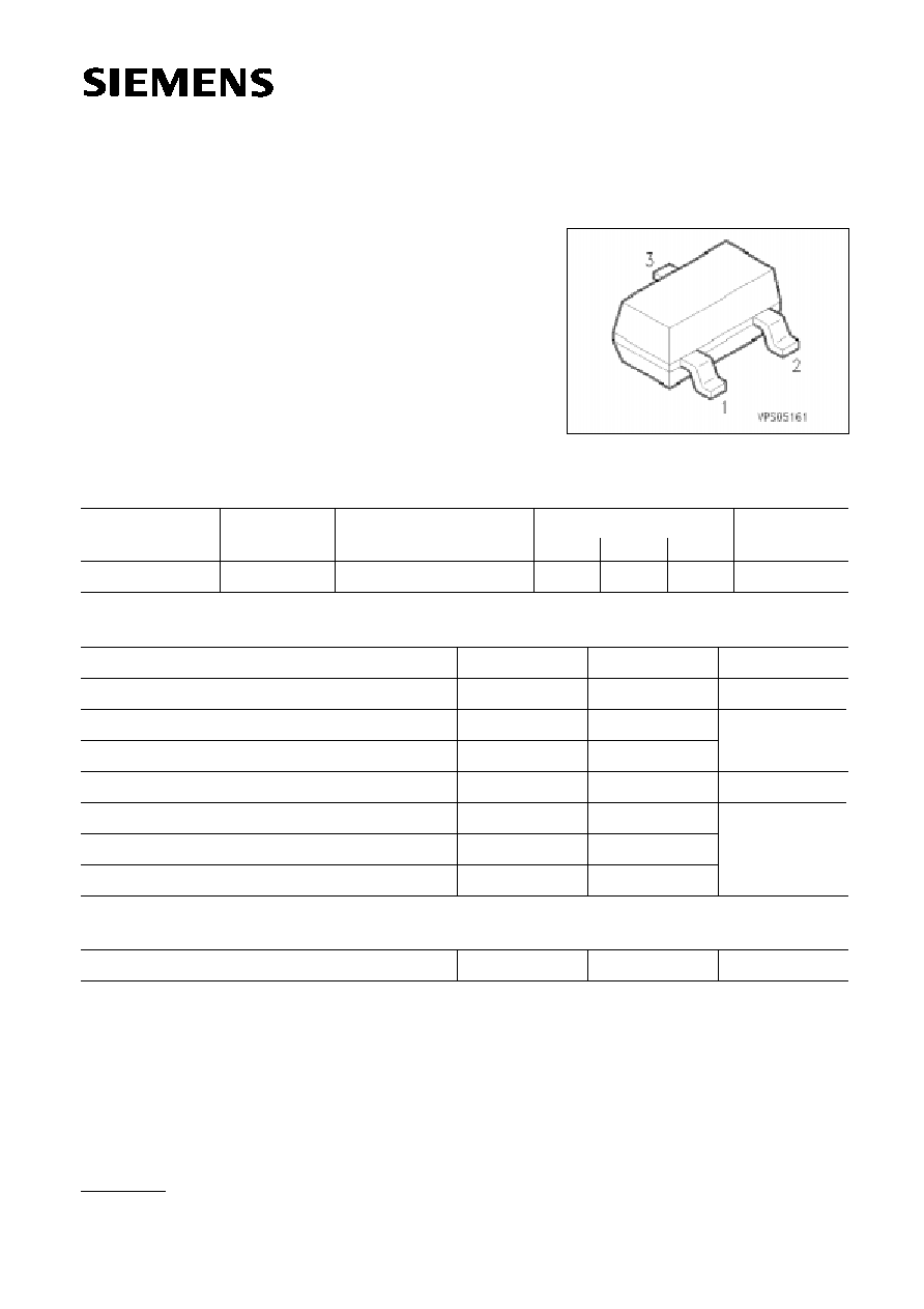
Package
1)
Pin Configuration
BF 543
Q62702-F1372
LDs
SOT-23
1
2
3
G
D
S
Thermal Resistance
Junction - ambient
2)
R
th JA
450
K/W
Parameter
Symbol
Values
Unit
Drain-source voltage
V
DS
20
V
Drain current
I
D
30
mA
Gate-source peak current
�
I
GSM
10
Total power dissipation,
T
A
60 �C
P
tot
200
mW
Storage temperature range
T
stg
� 55 ... + 150
�C
Channel temperature
T
ch
150
Ambient temperature range
T
A
� 55 ... + 150
1)
For detailed information see chapter Package Outlines.
2)
Package mounted on alumina 15 mm
�
16.7 mm
�
0.7 mm.
07.94

Semiconductor Group
2
Electrical Characteristics
at
T
A
= 25 �C, unless otherwise specified.
Unit
Values
V
nA
Parameter
Drain-source breakdown voltage
I
D
= 10
�
A, �
V
GS
= 4 V
Gate-source breakdown voltage
�
I
GS
= 10 mA,
V
DS
= 0
Gate cutoff current
�
V
GS
= 6 V,
V
DS
= 0
Symbol
V
(BR)DS
�
V
(BR)GSS
�
I
GSS
min.
20
7
�
typ.
�
�
�
max.
�
12
50
mA
Drain current
V
DS
= 10 V,
V
GS
= 0
I
DSS
2.0
4
6.0
V
Gate-source pinch-off voltage
V
DS
= 10 V,
I
D
= 20
�
A
�
V
GS(p)
�
0.7
1.5
DC Characteristics
mS
Forward transconductance
V
DS
= 10 V,
I
D
= 4 mA,
f
= 1 kHz
g
fs
9.5
12
�
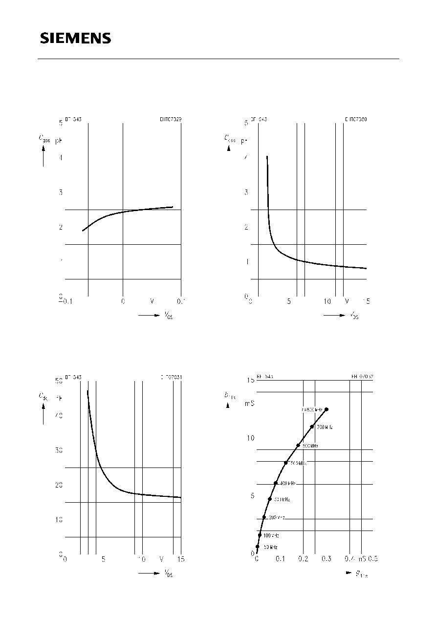
pF
Gate-1 input capacitance
V
DS
= 10 V,
I
D
= 4 mA,
f
= 1 MHz
C
gss
�
2.7
�
fF
Reverse transfer capacitance
V
DS
= 10 V,
I
D
= 4 mA,
f
= 1 MHz
C
dg
�
18
�
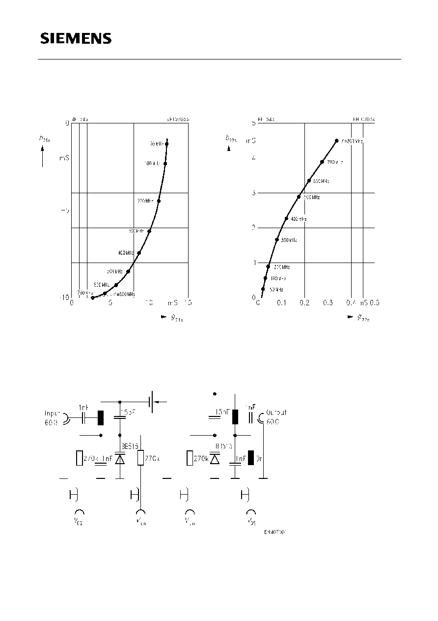
dB
Power gain (test circuit)
V
DS
= 10 V,
I
D
= 4 mA,
f
= 200 MHz
G
G
= 2 mS,
G
L
= 0.5 mS
G
p
�
22
�
pF
Output capacitance
V
DS
= 10 V,
I
D
= 4 mA,
f
= 1 MHz
C
dss
�
0.9
�
Noise figure (test circuit)
V
DS
= 10 V,
I
D
= 4 mA,
f
= 200 MHz
G
G
= 2 mS,
G
L
= 0.5 mS
F
�
1
�
AC Characteristics
BF 543