
GaAs MMIC
CF 750
_________________________________________________________________________________________
_______________
Siemens Aktiengesellschaft
pg. 1/6
12.01.96
HL EH PD 21
D a t a s h e e t
* Biased Dual Gate GaAs FET
* For frequencies from 400 MHz to 3 GHz
* Mixer and amplifier applications in handheld
equipment
* Low power consumption,
2mA operating current typ.
* Operating voltage range: 3 to 6V
* Ion-implanted planar structure
ESD: Electrostatic discharge sensitive device,
observe handling precautions!
Type
Marking
Ordering code
(taped)
Pin Configuration
1 2 3 4
Package 1)
CF 750
MX
Q62702-F1391
GND
D
G
S
SOT 143
Circuit diagram:
5k
G
D
S
20k
500
10pF
GND
Maximum ratings
Symbol
Unit
Drain-source voltage
VDS
8
V
Gate-source voltage
-VGS
5
V
Drain current
ID
80
mA
Gate-source peak current
+IGSM
2
mA
Channel temperature
TCh
150
�C
Storage temperature range
Tstg
-55 ... +150
�C
Total power dissipat. (T
S
<48�C)
2)
Ptot
300
mW
Thermal resistance
Channel-soldering point (GND)
RthChGND
340
K/W
1) For detailed
dimensions see chapter Package Outlines
2) T
S
: Temperature measured at soldering point

GaAs MMIC
CF 750
_________________________________________________________________________________________
_______________
Siemens Aktiengesellschaft
pg. 2/6
12.01.96
HL EH PD 21
Electrical characteristics
TA = 25�C, unless otherwise specified
DC characteristics
Symbol
min
typ
max
Unit
Drain-Source Breakdown Voltage
I
D
= 500
�
A, -V
GS
=4V
V
DS(BR)
8
-
-
V
Drain Current
V
GGND
= 0V, V
DS
= 3.8 V
S-pin not connected
I
DSS,P
1.6
2
2.8
mA
Drain Current
V
GS
= 0V, V
DS
= 3.8 V
S-pin connected to GND
I
DSS
-
50
-
mA
Transconductance
I
D
= 10 mA, V
DS
= 3.8 V
S-pin connected to GND
g
m
-
25
-
mS
Electrical characteristics of CF 750 in Amplifier Application
T
A
= 25 �C, V
DGND
= 3.8V, R
S
= R
L
= 50
,
unless otherwise specified
Amplifier Application
Symbol
min
typ
max
Unit
Power Gain
I
D
= 2 mA, f = 900 MHz
G
PS
-
11
-
dB
Noise Figure
I
D
= 2 mA, f = 900 MHz
F
-
1.6
-
dB
3rd Order Intermodulation
I
D
= 2 mA, f = 900 MHz
IPIP3
-
-1
-
dBm
3rd Order Intermodulation
I
D
= 2 mA, f = 900 MHz
OPIP3
-
10
-
dBm
Power Gain
I
D
= 2 mA, f = 1.8 GHz
G
PS
-
10
-
dB
Noise Figure
I
D
= 2 mA, f = 1.8 GHz
F
-
1.9
-
dB
3rd Order Intermodulation
I
D
= 2 mA, f = 1.8 GHz
IPIP3
-
-1
-
dBm
3rd Order Intermodulation
I
D
= 2 mA, f = 1.8 GHz
OPIP3
-
9
-
dBm

GaAs MMIC
CF 750
_________________________________________________________________________________________
_______________
Siemens Aktiengesellschaft
pg. 3/6
12.01.96
HL EH PD 21
Electrical characteristics of CF 750 in Mixer Application
T
A
= 25 �C, V
DGND
= 3.8V, R
S
= R
L
= 50
,
unless otherwise specified
Mixer Application
Symbol
min
typ
max
Unit
Single Sideband Noise Figure
f
RF
= 945 MHz, f
LO
= 900 MHz
f
IF
= 45 MHz, P
LO
= 3 dBm
F
SSB
-
4.5
-
dB
Conversion Gain
f
RF
= 945 MHz, f
LO
= 900 MHz
f
IF
= 45 MHz, P
LO
= 3 dBm
G
a
-
15
-
dB
3rd Order Intermodulation
f
RF
= 945 MHz, f
LO
= 900 MHz
f
IF
= 45 MHz, P
LO
= 3 dBm
IPIP3
-
-5
-
dBm
3rd Order Intermodulation
f
RF
= 945 MHz, f
LO
= 900 MHz
f
IF
= 45 MHz, P
LO
= 3 dBm
OPIP3
-
10
-
dBm
GaAs MMIC
CF 750
_________________________________________________________________________________________
_______________
Siemens Aktiengesellschaft
pg. 4/6
12.01.96
HL EH PD 21
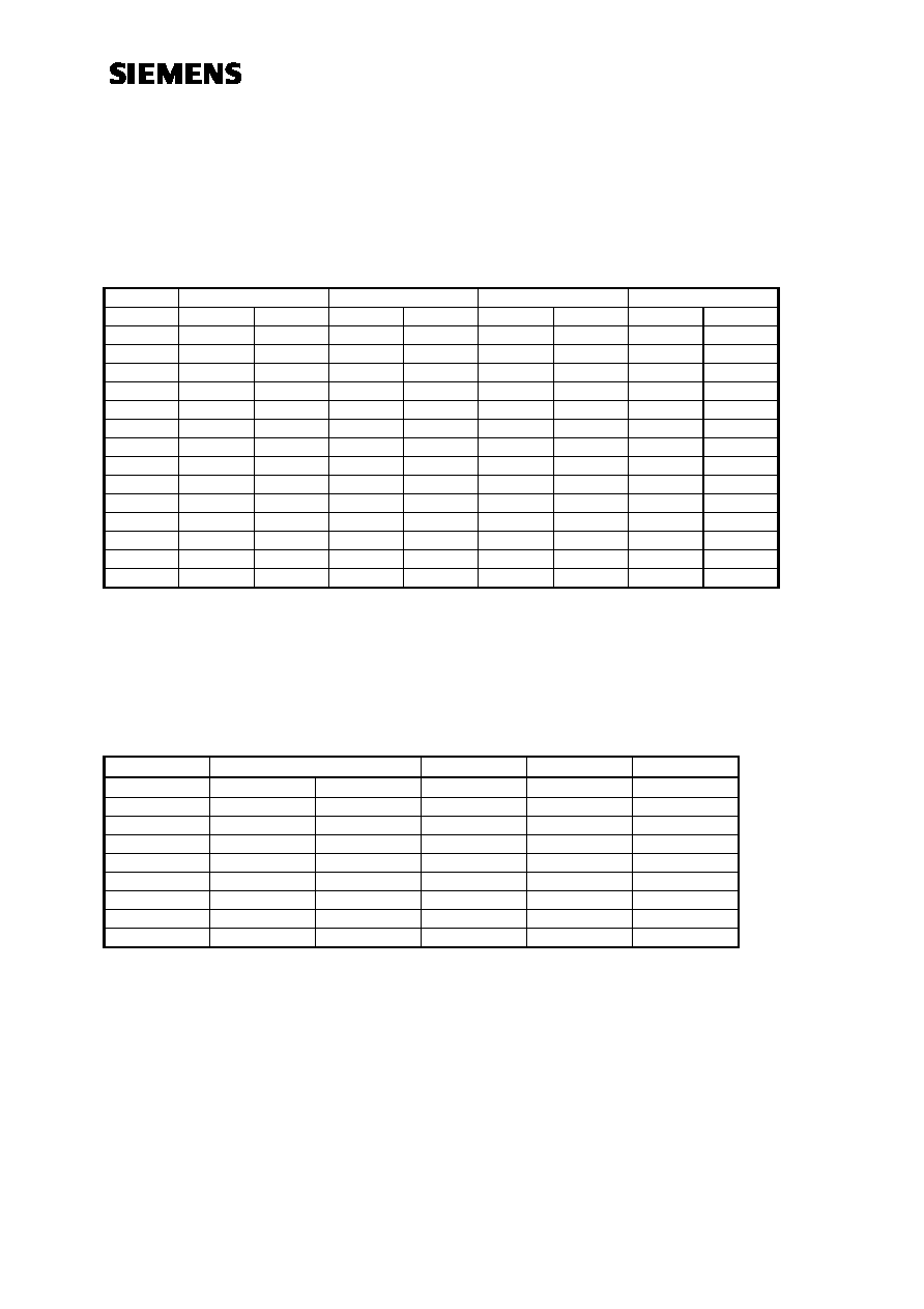
Typical Common Source S-Parameters
Bias conditions: V
DGND
= 3.8 V, I
D
= 2 mA
Source-Pad RF-grounded by capacitor with low inductance (< 0.5nH ) !
f
S11
S21
S12
S22
GHz
MAG
ANG
MAG
ANG
MAG
ANG
MAG
ANG
0.01
0.97
-1
1.78
179
0.002
89
0.98
-1
0.1
0.97
-3
1.78
175
0.008
84
0.98
-2
0.25
0.96
-8
1.76
169
0.015
78
0.97
-6
0.5
0.94
-16
1.73
155
0.027
75
0.95
-11
0.75
0.91
-26
1.70
141
0.039
71
0.93
-16
1.00
0.87
-34
1.68
127
0.046
64
0.91
-22
1.25
0.83
-42
1.65
118
0.052
62
0.89
-26
1.5
0.87
-49
1.62
108
0.061
57
0.88
-30
1.75
0.72
-57
1.59
95
0.066
55
0.87
-34
2.00
0.66
-65
1.54
82
0.069
52
0.86
-38
2.25
0.61
-73
1.51
71
0.071
54
0.85
-43
2.5
0.56
-81
1.47
60
0.073
60
0.84
-48
2.75
0.52
-87
1.45
52
0.074
63
0.83
-52
3.00
0.49
-93
1.42
45
0.075
66
0.82
-56
Typical Common Source Noise Parameters
Bias conditions: V
D
= 3 V, I
D
= 2 mA, Z = 50
f
opt
( F )
Rn
Rn/50
F min
MHz
MAG
ANG
-
dB
200
0.80
5
75
1.50
1.2
450
0.79
12
60
1.20
1.2
800
0.68
23
51
1.02
1.5
900
0.63
26
49
0.98
1.6
1200
0.58
34
45
0.90
1.7
1500
0.54
42
40
0.80
1.8
1800
0.52
51
36
0.72
1.9
1900
0.50
53
35
0.70
1.9

GaAs MMIC
CF 750
_________________________________________________________________________________________
_______________
Siemens Aktiengesellschaft
pg. 5/6
12.01.96
HL EH PD 21
Output characteristics I
D
= f (V
DGND
) at nominal operating point; S not
connected.
0
1 2 3 4 5 6 7 8
V
DGND
[V]
0.5
1.0
1.5
2.0
I
D
[mA]
V
GGND
= 0V
-0.2V
-0.4V
-0.6V
-0.8V
-1.0V
Output characteristics I
D
= f (V
DS
), S connected to GND.
0
1 2 3 4 5 6 7 8
0
10
20
30
40
50
I
D
[mA]
V
GS
=0V
V
GS
=-0.2V
V
GS
=-0.4V
V
GS
=-0.6V
V
GS
=-0.8V
V
GS
=-1.0V
V
DS
[V]