Semiconductor Group
1
Dec-12-1996
BFP 180W
NPN Silicon RF Transistor
∑ For low-power amplifiers in mobile
communication systems (pager) at collector
currents from 0.2 to 2.5mA
f
T
= 7GHz
∑
F = 2.1dB at 900MHz
ESD: Electrostatic discharge sensitive device, observe handling precaution!
Type
Marking Ordering Code
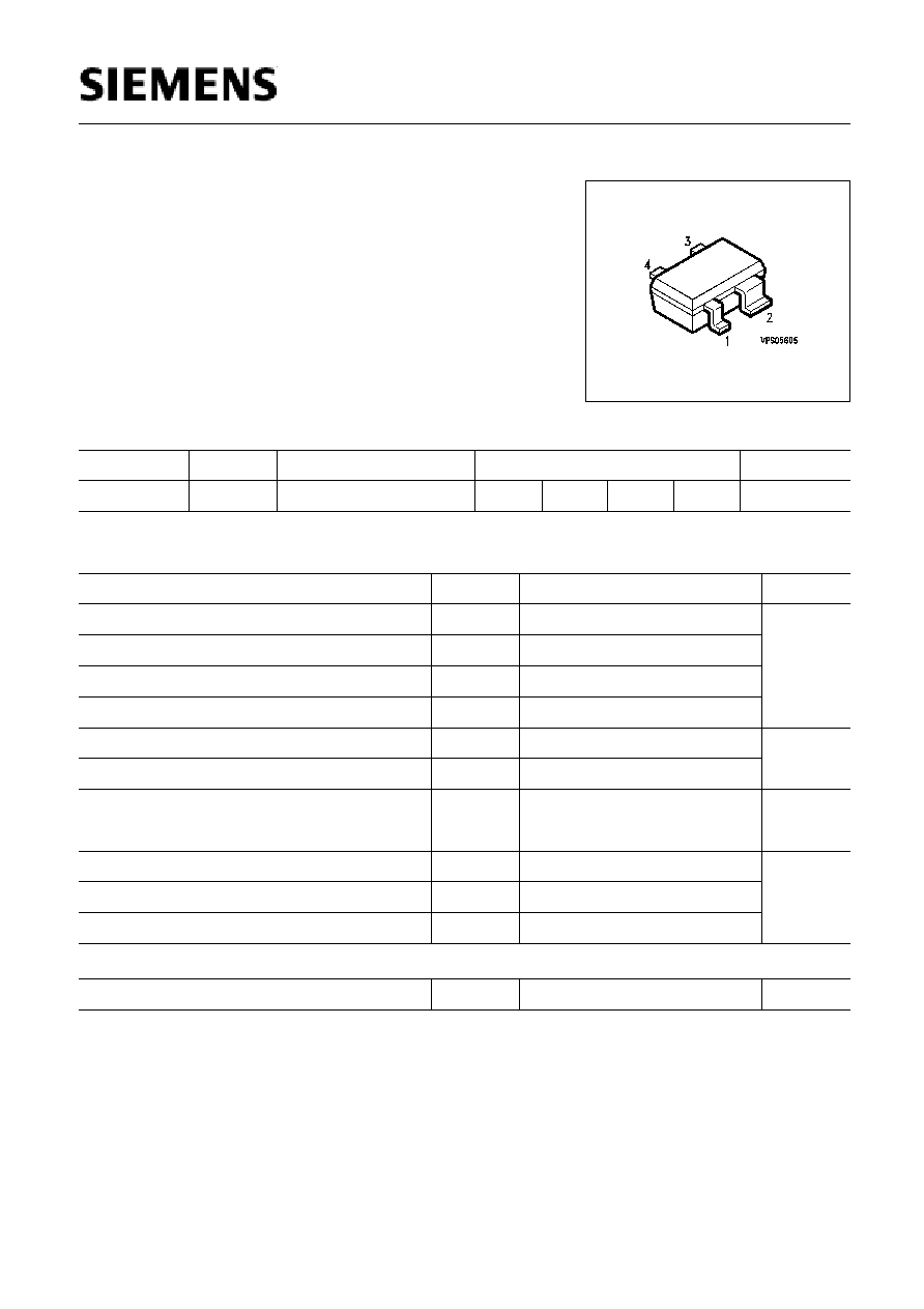
Pin Configuration
Package
BFP 180W
RDs
Q62702-F1500
1 = E
2 = C
3 = E
4 = B
SOT-343
Maximum Ratings
Parameter
Symbol
Values
Unit
Collector-emitter voltage
V
CEO
8
V
Collector-emitter voltage
V
CES
10
Collector-base voltage
V
CBO
10
Emitter-base voltage
V
EBO
2
Collector current
I
C
4
mA
Base current
I
B
0.5
Total power dissipation
T
S
126 ∞C
P
tot
30
mW
Junction temperature
T
j
150
∞C
Ambient temperature
T
A
- 65 ... + 150
Storage temperature
T
stg
- 65 ... + 150
Thermal Resistance
Junction - soldering point
1)
R
thJS
785
K/W
1)
T
S
is measured on the collector lead at the soldering point to the pcb.

Semiconductor Group
2
Dec-12-1996
BFP 180W
Electrical Characteristics at
T
A
= 25∞C, unless otherwise specified.
Parameter
Symbol
Values
Unit
min.
typ.
max.
DC Characteristics
Collector-emitter breakdown voltage
I
C
= 1 mA,
I
B
= 0
V
(BR)CEO
8
-
-
V
Collector-emitter cutoff current
V
CE
= 10 V,
V
BE
= 0
I
CES
-
-
100
µA
Collector-base cutoff current
V
CB
= 8 V,
I
E
= 0
I
CBO
-
-
100
nA
Emitter-base cutoff current
V
EB
= 1 V,
I
C
= 0
I
EBO
-
-
1
µA
DC current gain
I
C
= 1 mA,
V
CE
= 5 V
h
FE
30
100
200
-

Semiconductor Group
3
Dec-12-1996
BFP 180W
Electrical Characteristics at
T
A
= 25∞C, unless otherwise specified.
Parameter
Symbol
Values
Unit
min.
typ.
max.
AC Characteristics
Transition frequency
I
C
= 3 mA,
V
CE
= 5 V,
f = 500 MHz
f
T
5
7
-
GHz
Collector-base capacitance
V
CB
= 5 V,
f = 1 MHz
C
cb
-
0.22
0.35
pF
Collector-emitter capacitance
V
CE
= 5 V,
f = 1 MHz
C
ce
-
0.27
-
Emitter-base capacitance
V
EB
= 0.5 V,
f = 1 MHz
C
eb
-
0.1
-
Noise figure
I
C
= 1 mA,
V
CE
= 5 V,
Z
S
=
Z
Sopt
f = 900 MHz
f = 1.8 GHz
F
-
-
2.25
2.1
-
-
dB
Power gain
1)
I
C
= 1 mA,
V
CE
= 5 V,
Z
S
=
Z
Sopt
Z
L
=
Z
Lopt
f = 900 MHz
f = 1.8 GHz
G
ms
-
-
11.5
15
-
-
Transducer gain
I
C
= 1 mA,
V
CE
= 5 V,
Z
S
=
Z
L
= 50
f = 900 MHz
f = 1.8 GHz
|
S
21e
|
2
-
-
7
9
-
-
1)
G
ms
= |
S
21
/
S
12
|
Semiconductor Group
4
Dec-12-1996
BFP 180W
SPICE Parameters (Gummel-Poon Model, Berkeley-SPICE 2G.6 Syntax) :
Transistor Chip Data
IS =
0.18519
fA
VAF =
26.867
V
NE =
1.9818
-
VAR =
3.2134
V
NC =
1.6195
-
RBM =
60
CJE =
3.2473
fF
TF =
14.866
ps
ITF =
1.0202
mA
VJC =
1.1812
V
TR =
2.2648
ns
MJS =
0
-
XTI =
3
-
BF =
94.687
-
IKF =
0.025252
A
BR =
20.325
-
IKR =
0.012138
A
RB =
1.4255
RE =
3.7045
VJE =
1.1812
V
XTF =
0.3062
-
PTF =
0
deg
MJC =
0.30423
-
CJS =
0
fF
XTB =
0
-
FC =
0.87906
-
NF =
1.0236
-
ISE =
130.93
fA
NR =
0.93013
-
ISC =
6.1852
fA
IRB =
0.01
mA
RC =
0.56
MJE =
0.41827
-
VTF =
0.22023
V
CJC =
183.69
fF
XCJC =
0.08334
-
VJS =
0.75
V
EG =
1.11
eV
TNOM
300
K
All parameters are ready to use, no scalling is necessary.
Extracted on behalf of SIEMENS Small Signal Semiconductors by:
Institut f¸r Mobil-und Satellitenfunktechnik (IMST)
© 1996 SIEMENS AG
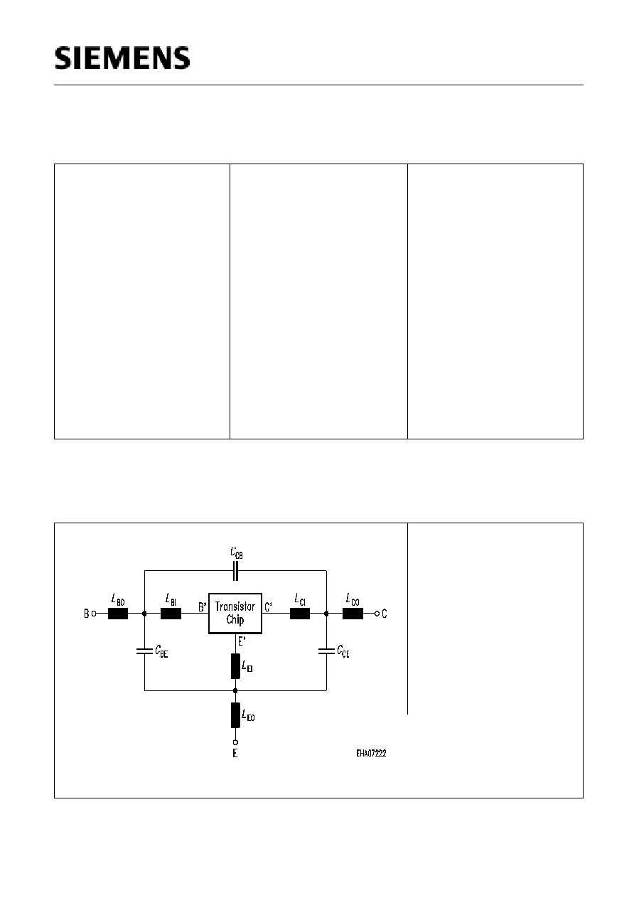
Package Equivalent Circuit:
LBI =
0.43
nH
LBO =
0.47
nH
LEI =
0.26
nH
LEO =
0.12
nH
LCI =
0.06
nH
LCO =
-
nH
CBE =
68
fF
CCB =
46
fF
CCE =
232
fF
Valid up to 6 GHz
For examples and ready to use parameters please contact your local Siemens distributor or sales office to
obtain a Siemens CD-ROM or see Internet: http://www.siemens.de/Semiconductor/products/35/35.htm
Semiconductor Group
5
Dec-12-1996
BFP 180W
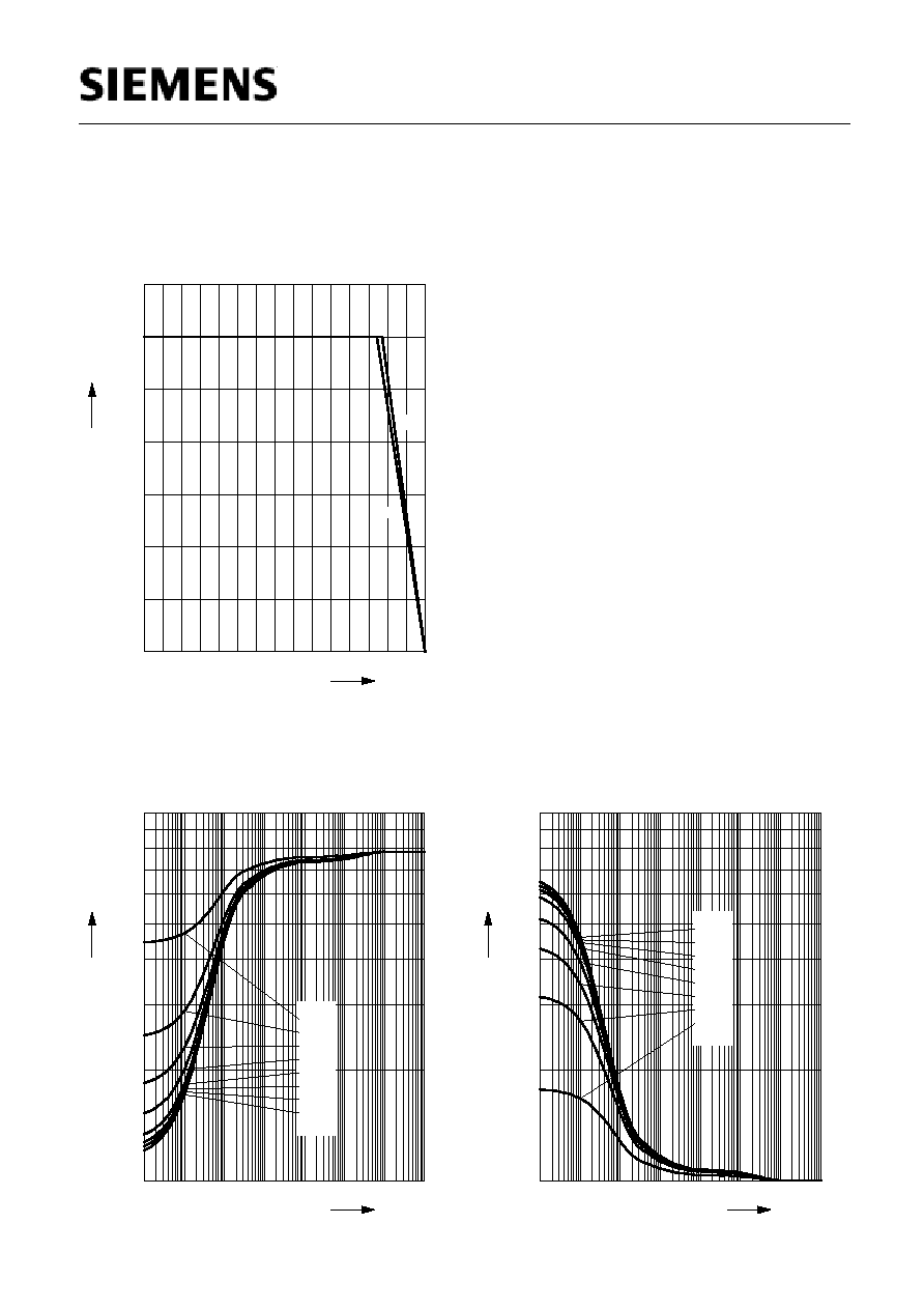
Total power dissipation
P
tot
=
f (T
A
*,
T
S
)
* Package mounted on epoxy
0
20
40
60
80
100
120 ∞C 150
T
A
,T
S
0
5
10
15
20
25
mW
35
P
tot
T
S
T
A
Permissible Pulse Load
R
thJS
=
f (t
p
)
10
-7
10
-6
10
-5
10
-4
10
-3
10
-2
10
-1
10
0
s
t
p
2
10
3
10
K/W
R
thJS
D = 0
0.005
0.01
0.02
0.05
0.1
0.2
0.5
Permissible Pulse Load
P
totmax
/
P
totDC
=
f (t
p
)
10
-7
10
-6
10
-5
10
-4
10
-3
10
-2
10
-1
10
0
s
t
p
0
10
1
10
-
P
totmax
/
P
totDC
D = 0
0.005
0.01
0.02
0.05
0.1
0.2
0.5
Semiconductor Group
6
Dec-12-1996
BFP 180W
Collector-base capacitance
C
cb
=
f (V
CB
)
V
BE
=
v
be
= 0,
f = 1MHz
0
2
4
6
8
V
12
V
R
0.0
0.1
0.2
0.3
pF
0.5
C
cb
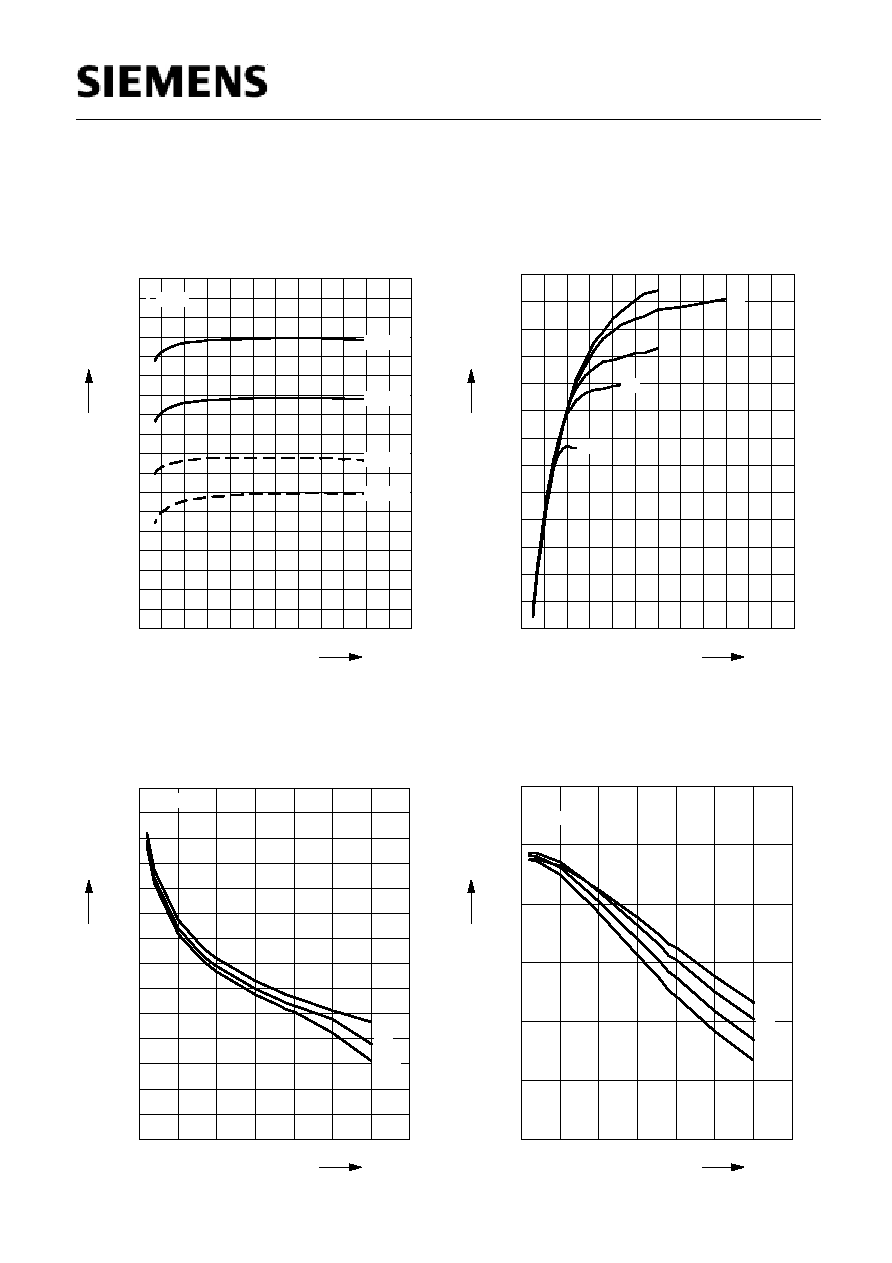
Transition frequency
f
T
=
f (I
C
)
V
CE
= Parameter
0.0 0.5 1.0 1.5 2.0 2.5 3.0 3.5 4.0 mA 5.0
I
C
0
1
2
3
4
5
6
7
8
GHz
10
f
T
10V
8V
5V
3V
2V
1V
0.7V
Power Gain
G
ma
,
G
ms
=
f(I
C
)
f = 0.9GHz
V
CE
= Parameter
0.0 0.5 1.0 1.5 2.0 2.5 3.0 3.5 4.0 mA 5.0
I
C
0
2
4
6
8
10
12
14
16
dB
20
G
10V
2V
1V
0.7V
Power Gain
G
ma
,
G
ms
=
f(I
C
)
f = 1.8GHz
V
CE
= Parameter
0.0 0.5 1.0 1.5 2.0 2.5 3.0 3.5 4.0 mA 5.0
I
C
0
2
4
6
8
10
12
14
dB
18
G
10V
5V
3V
2V
1V
0.7V
Semiconductor Group
7
Dec-12-1996
BFP 180W
Power Gain
G
ma
,
G
ms
=
f(V
CE
):_____
|
S
21
|
2
=
f(V
CE
):---------
f = Parameter
0
2
4
6
8
V
12
V
CE
0
2
4
6
8
10
12
14
dB
18
G
0.9GHz
1.8GHz
0.9GHz
1.8GHz
I
C
=1mA
Intermodulation Intercept Point
IP
3
=
f(I
C
)
(3rd order, Output,
Z
S
=
Z
L
=50
)
V
CE
= Parameter,
f = 900MHz
0.0
1.0
2.0
3.0
4.0
mA
6.0
I
C
-18
-16
-14
-12
-10
-8
-6
-4
-2
0
2
4
dBm
8
IP
3
8V
5V
3V
2V
1V
Power Gain
G
ma
,
G
ms
=
f(f)
V
CE
= Parameter
0.0
0.5
1.0
1.5
2.0
2.5
GHz
3.5
f
0
2
4
6
8
10
12
14
16
18
20
22
24
dB
28
G
10V
1V
0.7V
I
C
=1mA
Power Gain |
S
21
|
2
=
f(f)
V
CE
= Parameter
0.0
0.5
1.0
1.5
2.0
2.5
GHz
3.5
f
0
2
4
6
8
dB
12
G
10V
2V
1V
0.7V
I
C
=1mA