BF 2000
Semiconductor Group
Au -03-1998
1
Silicon N Channel MOSFET Tetrode
Target data sheet
∑
Short-channel transistor
with high S/C quality factor
∑
For low-noise, gain-controlled
input stages up to 1 GHz
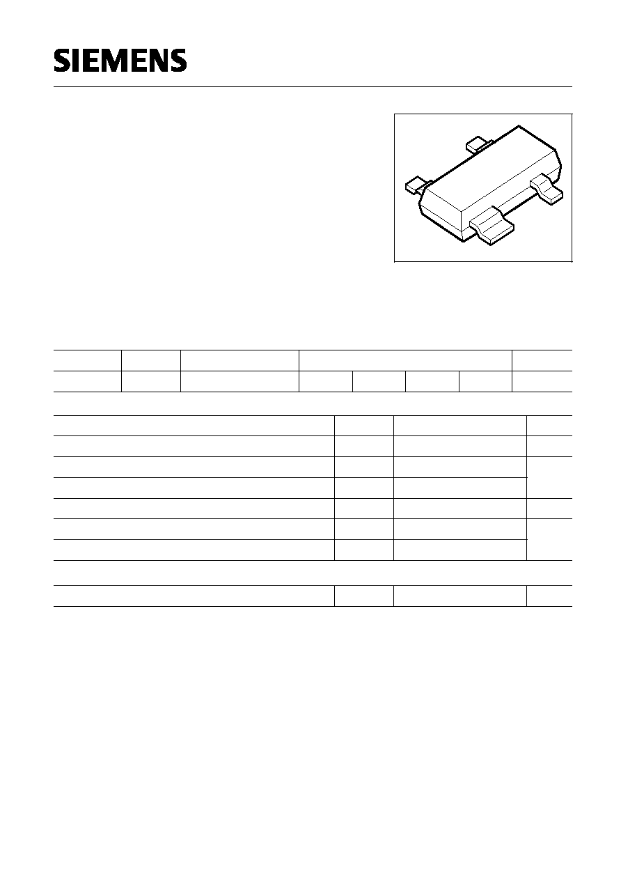
VPS05178
2
1
3
4
Package
Type
Marking Ordering Code
Pin Configuration
BF 2000
NDs
Q62702-F1771
4 = G1
SOT-143
1 = S
2 = D
3 = G2
Maximum Ratings
Parameter
Symbol
Unit
Value
V
DS
12
Drain-source voltage
V
30
I
D
mA
Continuos drain current
10
±
I
G1/2SM
Gate 1/gate 2 peak source current
Total power dissipation,
T
S
= 76 ∞C
mW
P
tot
200
Storage temperature
- 55 ...+150
∞C
T
stg
T
ch
150
Channel temperature
Thermal Resistance
370
K/W
Channel - soldering point
R
thchs
Semiconductor Group
1
1998-11-01
BF 2000
Semiconductor Group
Au -03-1998
2
Electrical Characteristics at
T
A
= 25 ∞C; unless otherwise specified.
Parameter
Symbol
Values
Unit
typ.
max.
min.
DC characteristics
Drain-source breakdown voltage
I
D
= 10 µA, -
V
G1S
= 4 V, -
V
G2S
= 4 V
V
(BR)DS
-
V
-
12
Gate 1 source breakdown voltage
±
I
G1S
= 10 mA,
V
G2S
=
V
DS
= 0
±
V
(BR)G1SS
8
12
V
-
±
V
(BR)G2SS
8
12
-
Gate 2 source breakdown voltage
±
I
G2S
= 10 mA,
V
G1S
= 0 V,
V
DS
= 0 V
nA
Gate 1 source leakage current
±
V
G1S
= 5 V,
V
G2S
=
V
DS
= 0
±
I
G1SS
-
-
50
Gate 2 source leakage current
±
V
G2S
= 5 V,
V
G1S
= 0 V,
V
DS
= 0 V
50
-
-
±
I
G2SS
µA
Drain current
V
DS
= 5 V,
V
G1S
= 0 ,
V
G2S
= 4 V
I
DSS
1
-
-
V
-
-
0.3
V
G1S(p)
Gate 1-source pinch-off voltage
V
DS
= 5 V,
V
G2S
= 4 V,
I
D
= 200 µA
V
Gate 2-source pinch-off voltage
V
DS
= 5 V,
I
D
= 100 µA
-
0.2
V
G2S(p)
-
Semiconductor Group
2
1998-11-01
BF 2000
Semiconductor Group
Au -03-1998
3
Electrical Characteristics at
T
A
= 25 ∞C, unless otherwise specified.
Parameter
Symbol
Values
Unit
min.
typ.
max.
AC characteristics
Forward transconductance
V
DS
= 5 V,
I
D
= 10 mA,
V
G2S
= 4 V,
f = 1 kHz
g
fs
-
24
-
mS
Gate 1 input capacitance
V
DS
= 5 V,
I
D
= 10 mA,
V
G2S
= 4 V,
f = 1 MHz
C
g1ss
-
1.2
-
pF
Gate 2 input capacitance
V
DS
= 5 V,
I
D
= 10 mA,
V
G2S
= 4 V,
f = 1 MHz
C
g2ss
-
-
-
Feedback capacitance
V
DS
= 8 V,
I
D
= 10 mA,
V
G2S
= 4 V,
f = 1 MHz
C
dg1
-
25
-
fF
Output capacitance
V
DS
= 5 V,
I
D
= 10 mA,
V
G2S
= 4 V,
f = 1 MHz
C
dss
-
0.8
-
pF
Power gain
V
DS
= 5 V,
I
D
= 10 mA,
V
G2S
= 4 V,
f = 45 MHz
G
ps
28
29
-
dB
Power gain
V
DS
= 5 V,
I
D
= 10 mA,
V
G2S
= 4 V,
f = 800 MHz
G
ps
-
22
-
Noise figure
V
DS
= 5 V,
I
D
= 10 mA,
V
G2S
= 4 V,
f = 45 MHz
F
-
1.1
-
Noise figure
V
DS
= 5 V,
I
D
= 10 mA,
V
G2S
= 4 V,
f = 800 MHz
F
-
1
-
Gain control range
V
DS
= 8 V, VG2S = 4 ... -2V,
f = 800 MHz
G
ps
40
-
-
Semiconductor Group
3
1998-11-01