Semiconductor Group
1
Aug-14-1996
BF 660W
PNP Silicon RF Transistor
∑ For VHF oscillator applications
Type
Marking Ordering Code
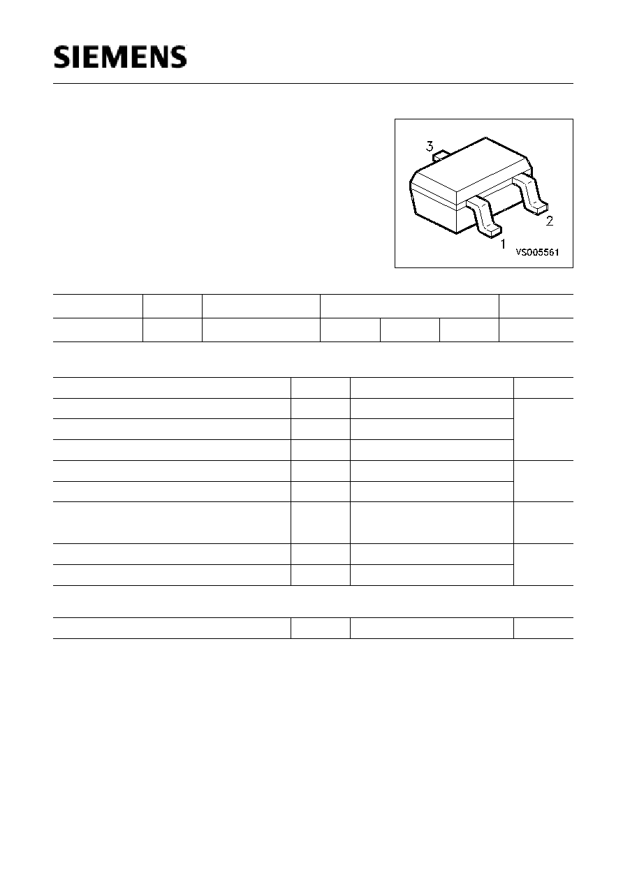
Pin Configuration
Package
BF 660W
LEs
Q62702-F1568
1 = B
2 = E
3 = C
SOT-323
Maximum Ratings
Parameter
Symbol
Values
Unit
Collector-emitter voltage
V
CEO
30
V
Collector-base voltage
V
CBO
40
Emitter-base voltage
V
EBO
4
Collector current
I
C
25
mA
Base current
I
B
5
Total power dissipation
T
S
93 ∞C
P
tot
280
mW
Junction temperature
T
j
150
∞C
Storage temperature
T
stg
- 65 ... + 150
Thermal Resistance
Junction - soldering point
R
thJS
205
K/W

Semiconductor Group
2
Aug-14-1996
BF 660W
Electrical Characteristics at
T
A
= 25∞C, unless otherwise specified.
Parameter
Symbol
Values
Unit
min.
typ.
max.
DC Characteristics
Collector-emitter breakdown voltage
I
C
= 1 mA,
I
B
= 0
V
(BR)CEO
30
-
-
V
Collector-base breakdown voltage
I
C
= 10 µA,
I
E
= 0
V
(BR)CBO
40
-
-
Base-emitter breakdown voltage
I
E
= 10 µA,
I
C
= 0
V
(BR)EBO
4
-
-
Collector-base cutoff current
V
CB
= 20 ,
I
E
= 0
I
CBO
-
-
50
nA
DC current gain
I
C
= 3 mA,
V
CE
= 10 V
h
FE
30
-
-
-
AC Characteristics
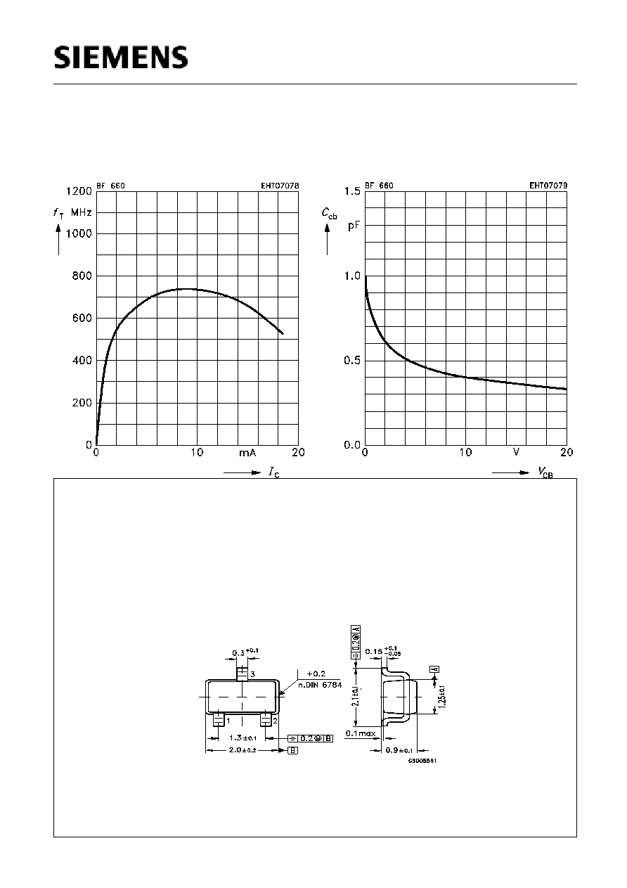
Transition frequency
I
C
= 5 mA,
V
CE
= 10 V,
f = 100 MHz
f
T
-
700
-
MHz
Collector-base capacitance
V
CB
= 10 V,
V
BE
=
v
be
= 0 ,
f = 1 MHz
C
cb
-
0.4
-
pF
Collector-emitter capacitance
V
CE
= 10 V,
V
BE
=
v
be
= 0 ,
f = 1 MHz
C
ce
-
0.15
-