Semiconductor Group
1
Nov-28-1996
BF 799W
NPN Silicon RF Transistor
∑ For linear broadband amplifier applications
up to 500MHz
∑ SAW filter driver in TV tuners
Type
Marking Ordering Code
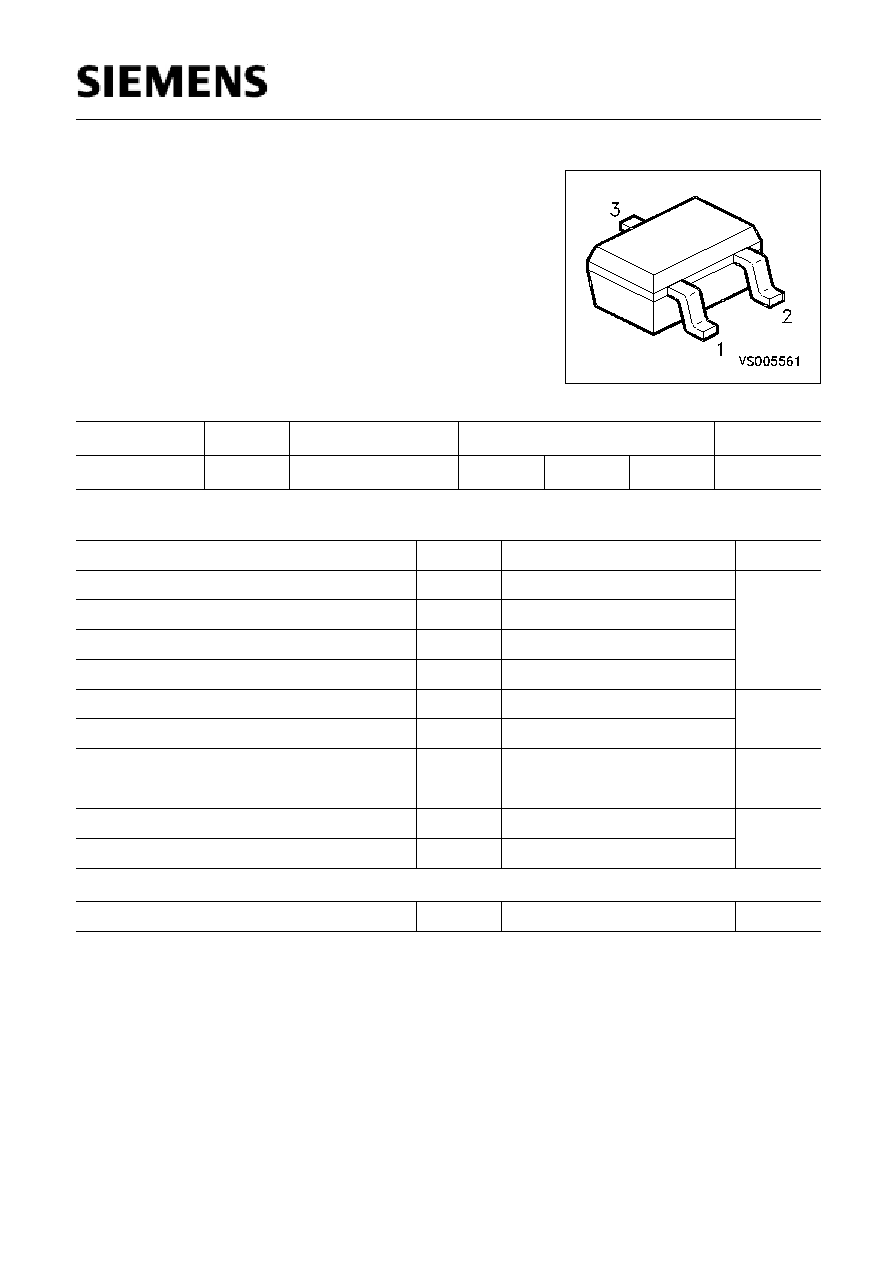
Pin Configuration
Package
BF 799W
LKs
Q62702-F1571
1 = B
2 = E
3 = C
SOT-323
Maximum Ratings
Parameter
Symbol
Values
Unit
Collector-emitter voltage
V
CEO
20
V
Collector-emitter voltage
V
CES
30
Collector-base voltage
V
CBO
30
Emitter-base voltage
V
EBO
3
Collector current
I
C
35
mA
Base current
I
B
10
Total power dissipation
T
S
107 ∞C
P
tot
280
mW
Junction temperature
T
j
150
∞C
Storage temperature
T
stg
- 65 ... - 150
Thermal Resistance
Junction - soldering point
R
thJS
155
K/W

Semiconductor Group
2
Nov-28-1996
BF 799W
Electrical Characteristics at
T
A
= 25∞C, unless otherwise specified.
Parameter
Symbol
Values
Unit
min.
typ.
max.
DC Characteristics
Collector-emitter breakdown voltage
I
C
= 1 mA,
I
B
= 0
V
(BR)CEO
20
-
-
V
Collector-base breakdown voltage
I
C
= 10 µA,
I
E
= 0
V
(BR)CBO
30
-
-
Base-emitter breakdown voltage
I
E
= 10 µA,
I
C
= 0
V
(BR)EBO
3
-
-
Collector-base cutoff current
V
CB
= 20 V,
I
E
= 0
I
CBO
-
-
100
nA
DC current gain
I
C
= 5 mA,
V
CE
= 10 V
I
C
= 20 mA,
V
CE
= 10 V
h
FE
40
35
100
95
250
-
-
Collector-emitter saturation voltage
I
C
= 20 mA,
I
B
= 2 mA
V
CEsat
-
0.15
0.5
V
Base-emitter saturation voltage
I
C
= 20 mA,
I
B
= 2 mA
V
BEsat
-
-
0.95

Semiconductor Group
3
Nov-28-1996
BF 799W
Electrical Characteristics at
T
A
= 25∞C, unless otherwise specified.
Parameter
Symbol
Values
Unit
min.
typ.
max.
AC Characteristics
Transition frequency
I
C
= 5 mA,
V
CE
= 10 V,
f = 100 MHz
I
C
= 20 mA,
V
CE
= 8 V,
f = 100 MHz
f
T
-
-
1100
800
-
-
MHz
Collector-base capacitance
V
CB
= 10 V,
V
BE
=
v
be
= 0 ,
f = 1 MHz
C
cb
-
0.7
-
pF
Collector-emitter capacitance
V
CE
= 10 V,
V
BE
=
v
be
= 0 ,
f = 1 MHz
C
ce
-
0.28
-
Output capacitance
V
CB
= 10 V,
I
E
= 0 mA,
f = 1 MHz
C
ob
-
0.96
-
Noise figure
I
C
= 5 mA,
V
CE
= 10 V,
f = 100 MHz
Z
S
= 50
F
-
3
-
dB
Output conductance
I
C
= 20 mA,
V
CE
= 10 V,
f = 35 MHz
g
22e
-
60
-
µS

Semiconductor Group
4
Nov-28-1996
BF 799W
Total power dissipation
P
tot
=
f (T
A
*,
T
S
)
* Package mounted on epoxy
0
20
40
60
80
100
120 ∞C 150
T
A
,T
S
0
20
40
60
80
100
120
140
160
180
200
220
240
260
mW
300
P
tot
T
S
T
A
Permissible Pulse Load
R
thJS
=
f (t
p
)
10
-7
10
-6
10
-5
10
-4
10
-3
10
-2
10
-1
10
0
s
t
p
0
10
1
10
2
10
3
10
K/W
R
thJS
D = 0
0.005
0.01
0.02
0.05
0.1
0.2
0.5
Permissible Pulse Load
P
totmax
/
P
totDC
=
f (t
p
)
10
-7
10
-6
10
-5
10
-4
10
-3
10
-2
10
-1
10
0
s
t
p
0
10
1
10
2
10
-
P
totmax
/
P
totDC
D = 0
0.005
0.01
0.02
0.05
0.1
0.2
0.5

Semiconductor Group
5
Nov-28-1996
BF 799W
Transition frequency
f
T
=
f (I
C
)
f = 100MHz
V
CE
= Parameter
Collector-base capacitance
C
cb
=
f (V
CB
)
V
BE
=
v
be
= 0,
f = 1MHz