
BFP 405
Semiconductor Group
Sep-09-1998
1
SIEGET
Æ
25
NPN Silicon RF Transistor
∑
For low current applications
∑
For oscillators up to 12 GHz
∑
Noise figure
F = 1.15 dB at 1.8 GHz
outstanding
G
ms
= 22 dB at 1.8 GHz
∑
Transition frequency
f
T
= 25 GHz
∑
Gold metalization for high reliability
∑
SIEGET
Æ
25 - Line
Siemens Grounded Emitter Transistor
25 GHz
f
T
- Line
VPS05605
4
2
1
3
ESD: Electrostatic discharge sensitive device, observe handling precaution!
Type
Marking Ordering Code
Pin Configuration
Package
BFP 405
ALs
Q62702-F1592
1 = B
2 = E
3 = C
4 = E
SOT-343
Maximum Ratings
Parameter
Symbol
Value
Unit
Collector-emitter voltage
V
CEO
V
4.5
V
CBO
15
Collector-base voltage
V
EBO
Emitter-base voltage
1.5
Collector current
12
mA
I
C
I
B
1
Base current
mW
55
Total power dissipation,
T
S
120 ∞C
P
tot
Junction temperature
T
j
150
∞C
T
A
-65 ...+150
Ambient temperature
Storage temperature
T
stg
-65 ...+150
Thermal Resistance
Junction - soldering point
1)
R
thJS
530
K/W
1) TS is measured on the collector lead at the soldering point to the pcb
Semiconductor Group
1
1998-11-01

BFP 405
Semiconductor Group
Sep-09-1998
2
Electrical Characteristics at
T
A
= 25∞C, unless otherwise specified.
Parameter
Symbol
Values
Unit
min.
typ.
max.
DC characteristics
5
6.5
4.5
V
(BR)CEO
Collector-emitter breakdown voltage
I
C
= 1 mA,
I
B
= 0
V
-
150
-
Collector-base cutoff current
V
CB
= 5 V,
I
E
= 0
I
CBO
nA
-
15
µA
-
Emitter-base cutoff current
V
EB
= 1.5 V,
I
C
= 0
I
EBO
90
DC current gain
I
C
= 5 mA,
V
CE
= 4 V
h
FE
150
-
50
AC characteristics
Transition frequency
I
C
= 10 mA,
V
CE
= 3 V,
f = 2 GHz
f
T
20
25
-
GHz
Collector-base capacitance
V
CB
= 2 V,
f = 1 MHz
C
cb
-
0.05
0.08
pF
Collector-emitter capacitance
V
CE
= 2 V,
f = 1 MHz
C
ce
-
0.28
-
Emitter-base capacitance
V
EB
= 0.5 V,
f = 1 MHz
C
eb
-
0.29
-
Noise figure
I
C
= 2 mA,
V
CE
= 2 V,
Z
S
=
Z
Sopt
,
f = 900 MHz
F
-
1.15
1.4
dB
Power gain
1)
I
C
= 5 mA,
V
CE
= 2 V,
Z
S
=
Z
Sopt
,
Z
L
=
Z
Lopt
,
f = 1.8 GHz
G
ms
-
22
-
Insertion power gain
I
C
= 5 mA,
V
CE
= 2 V,
f = 1.8 GHz,
Z
S
=
Z
L
= 50
|
S
21
|
2
14
17
-
dB
Third order intersept point
I
C
= 5 mA,
V
CE
= 2 V,
Z
S
=
Z
Sopt
,
Z
L
=
Z
Lopt
,
f = 1.8 GHz
IP
3
-
15
-
dBm
1dB Compression point
I
C
= 5 mA,
V
CE
= 2 V,
f = 1.8 GHz,
Z
S
=
Z
Sopt
,
Z
L
=
Z
Lopt
P
-1dB
-
5
-
1)
Gms = |S21 / S12|
Semiconductor Group
2
1998-11-01

BFP 405
Semiconductor Group
Sep-09-1998
3
Common Emitter S-Parameters
f
S
11
S
21
S
12
S
22
GHz
MAG
ANG
MAG
ANG
MAG
ANG
MAG
ANG
V
CE
= 2V,
I
C
= 5mA
0.1
0.5
1
2
3
4
6
8
9
10
11
12
0.841
0.791
0.682
0.449
0.304
0.239
0.303
0.464
0.549
0.631
0.666
0.693
-5.2
-25.4
-48.7
-88.6
-126.1
-171.1
129.3
91.4
77.9
71
67.6
63.4
13.52
12.76
11.25
8.04
5.91
4.63
3.13
2.22
1.93
1.65
1.47
1.23
174.9
154.6
133.3
100.3
77.4
58.9
28
-1.5
-15.5
-27.5
-38.2
-49.5
0.0033
0.0161
0.0290
0.0479
0.0639
0.799
0.1104
0.118
0.129
0.136
0.145
0.155
88.9
77.5
67.9
55.4
49.2
43.2
30.2
13.6
5.1
-2.2
-8.5
-15.3
0.986
0.956
0.873
0.709
0.594
0.509
0.386
0.251
0.153
0.069
0.127
0.187
-2.5
-12.6
-22.7
-36.8
-44.7
-55.5
-73.5
-92.2
106.6
-166.6
137.2
75.6
Common Emitter Noise Parameters
f
F
min
1)
G
a
1)
opt
R
N
r
n
F
50
2)
|
S
21
|
2 2)
GHz
dB
dB
MAG
ANG
-
dB
dB
V
CE
= 2V,
I
C
= 2mA
0.9
1.8
2.4
3.0
4
5
6
0.9
1.15
1.35
1.46
1.62
1.75
2.15
21.2
18.2
15.5
14.5
11.9
9.3
8.1
0.54
0.46
0.41
0.34
0.26
0.17
0.13
14
27
38
55
80
117
180
21
19
18
17
12.5
11
14
0.42
0.38
0.36
0.34
0.25
0.22
0.28
1.8
1.8
1.8
1.8
1.8
1.9
2.2
16.1
15
14
12.9
11.3
9.7
8.2
1) Input matched for minimum noise figure, output for maximum gain 2)
Z
S
=
Z
L
= 50
For more and detailed S- and Noise-parameters please contact your local Siemens
distributor or sales office to obtain a Siemens Application Notes CD-ROM or see Internet:
http://www.siemens.de/Semiconductor/products/35/35.htm
Semiconductor Group
3
1998-11-01

BFP 405
Semiconductor Group
Sep-09-1998
4
SPICE Parameters (Gummel-Poon Model, Berkley-SPICE 2G.6 Syntax) :
Transistor Chip Data
IS =
0.21024
fA
VAF =
39.251
V
NE =
1.7763
-
VAR =
34.368
V
NC =
1.3152
-
RBM =
1.3491
CJE =
3.7265
fF
TF =
4.5899
ps
ITF =
1.3364
mA
VJC =
0.99532
V
TR =
1.4935
ns
MJS =
0
-
XTI =
3
-
NF =
1.0405
-
ISE =
15.761
fA
NR =
0.96647
-
ISC =
0.037223
fA
IRB =
0.21215
mA
RC =
0.12691
MJE =
0.37747
-
VTF =
0.19762
V
CJC =
96.941
fF
XCJC =
0.08161
-
VJS =
0.75
V
EG =
1.11
eV
TNOM
300
K
BF =
83.23
-
IKF =
0.16493
A
BR =
10.526
-
IKR =
0.25052
A
RB =
15
RE =
1.9289
VJE =
0.70367
V
XTF =
0.3641
-
PTF =
0
deg
MJC =
0.48652
-
CJS =
0
fF
XTB =
0
-
FC =
0.99469
-
C'-E'-Diode Data (Berkley-SPICE 2G.6 Syntax) :
IS =
2
fA
N =
1.02
-
RS =
20
All parameters are ready to use, no scalling is necessary
Package Equivalent Circuit:
L
BI
=
0.47
nH
L
BO
=
0.53
nH
L
EI
=
0.23
nH
L
EO
=
0.05
nH
L
CI
=
0.56
nH
L
CO
=
0.58
nH
C
BE
=
136
fF
C
CB
=
6.9
fF
C
CE
=
134
fF
EHA07389
L
BI
BE
C
BO
L
C
EI
L
L
EO
CB
C
CI
L
CO
L
CE
C
Transistor
C'-E'-
B
Diode
E
E'
C'
B'
Chip
Valid up to 6GHz
The SOT-343 package has two emitter leads. To avoid high complexity of the package equivalent circuit,
both leads are combined in one electrical connection.
Extracted on behalf of SIEMENS Small Signal Semiconductors by:
Institut f¸r Mobil-und Satellitentechnik (IMST)
©
1996 SIEMENS AG
For examples and ready to use parameters please contact your local Siemens distributor or sales office to
obtain a Siemens CD-ROM or see Internet: http://www.siemens.de/Semiconductor/products/35/35.htm
Semiconductor Group
4
1998-11-01
BFP 405
Semiconductor Group
Sep-09-1998
5
For non-linear simulation:
∑
Use transistor chip parameters in Berkeley SPICE 2G.6 syntax for all simulators.
∑
If you need simulation of thereverse characteristics, add the diode with the
C'-E'- diode data between collector and emitter.
∑
Simulation of package is not necessary for frequenties < 100MHz.
For higher frequencies add the wiring of package equivalent circuit around the
non-linear transistor and diode model.
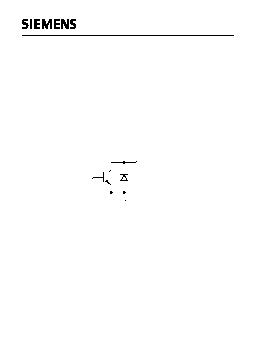
Note:
∑
This transistor is constructed in a common emitter configuration. This feature causes
an additional reverse biased diode between emitter and collector, which does not
effect normal operation.
EHA07307
C
E
E
B
Transistor Schematic Diagram
The common emitter configuration shows the following advantages:
∑
Higher gain because of lower emitter inductance.
∑
Power is dissipated via the grounded emitter leads, because the chip is mounted
on copper emitter leadframe.
Please note, that the broadest lead is the emitter lead.
The AC characteristics are verified by random sampling.
Semiconductor Group
5
1998-11-01