
BF 414
Semiconductor Group
1
NPN Silicon RF Transistor
BF 414
q
For low-noise, common base
VHF and FM stages
1
3
2
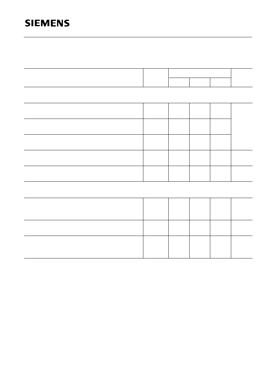
Maximum Ratings
Type
Ordering Code
Marking
Package
1)
Pin Configuration
BF 414
Q62702-F517
≠
TO-92
1
2
3
C
B
E
Parameter
Symbol
Values
Unit
Collector-emitter voltage
V
CE0
30
V
Collector-base voltage
V
CB0
40
Emitter-base voltage
V
EB0
4
Thermal Resistance
Junction - ambient
R
th JA
350
K/W
Collector current
I
C
25
mA
Base current
I
B
3
Total power dissipation,
T
A
45 ∞C
P
tot
300
mW
Junction temperature
T
j
150
∞C
Storage temperature range
T
stg
≠ 55 ... + 150
1)
For detailed information see chapter Package Outlines.
BF 414
Semiconductor Group
2
Electrical Characteristics
at
T
A
= 25 ∞C, unless otherwise specified.
DC Characteristics
MHz
Transition frequency
I
C
= 1 mA,
V
CE
= 10 V,
f
= 100 MHz
I
C
= 5 mA,
V
CE
= 10 V,
f
= 100 MHz
f
T
≠
≠
400
560
≠
≠
dB
Noise figure
I
C
= 5 mA,
V
CE
= 10 V,
f
= 100 MHz
R
S
= 60
F
≠
3
≠
pF
Collector-emitter capacitance
V
CE
= 10 V,
V
BE
= 0 V,
f
= 1 MHz
C
ce
≠
0.1
≠
Unit
Values
V
Parameter
Collector-emitter breakdown voltage
I
C
= 2 mA,
I
B
= 0
Collector-base breakdown voltage
I
C
= 10
µ
A,
I
E
= 0
Emitter-base breakdown voltage
I
E
= 10
µ
A
Symbol
V
(BR) CE0
V
(BR) CB0
V
(BR) EB0
min.
30
40
4
typ.
≠
≠
≠
max.
≠
≠
≠
nA
Collector cutoff current
V
CB
= 20 V
I
CB0
≠
≠
60
≠
DC current gain
I
C
= 4 mA,
V
CE
= 10 V
h
FE
30
80
≠
AC Characteristics