Semiconductor Group
1
NPN Silicon High-Voltage Transistors
BFN 16
BFN 18
Maximum Ratings
Type
Ordering Code
(tape and reel)
Marking
Package
1)
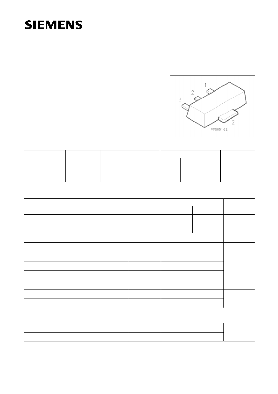
Pin Configuration
BFN 16
BFN 18
Q62702-F885
Q62702-F1056
DD
DE
SOT-89
1
2
3
B
C
E
1)
For detailed information see chapter Package Outlines.
2)
Package mounted on epoxy pcb 40 mm
◊
40 mm
◊
1.5 mm/6 cm
2
Cu.
Parameter
Symbol
BFN 16
Unit
Collector-emitter voltage
V
CE0
250
V
Collector-base voltage
V
CB0
250
Emitter-base voltage
V
EB0
Collector current
I
C
mA
Base current
I
B
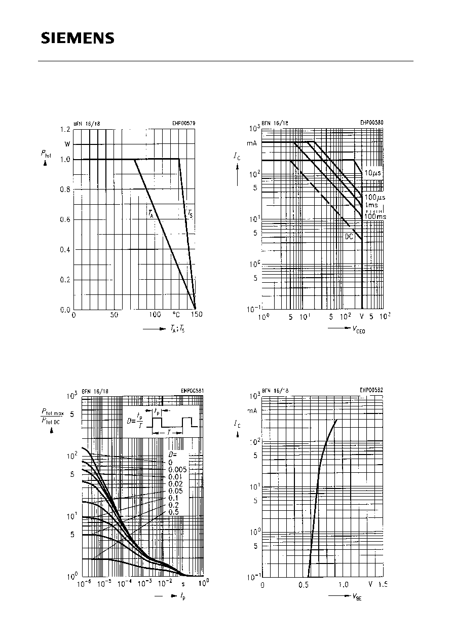
Total power dissipation,
T
S
= 130 ∞C
P
tot
W
Junction temperature
T
j
∞C
Storage temperature range
T
stg
≠ 65 ... + 150
Thermal Resistance
Junction - ambient
2)
R
th JA
75
K/W
Peak collector current
I
CM
Peak base current
I
BM
BFN 18
300
300
200
100
1
150
500
200
Values
5
Junction - soldering point
R
th JS
20
q
Suitable for video output stages in TV sets
and switching power supplies
q
High breakdown voltage
q
Low collector-emitter saturation voltage
q
Complementary types: BFN 17, BFN 19 (PNP)
5.91
Semiconductor Group
2
BFN 16
BFN 18
Electrical Characteristics
at
T
A
= 25 ∞C, unless otherwise specified.
Base-emitter saturation voltage
1)
I
C
= 20 mA,
I
B
= 2 mA
Collector-emitter saturation voltage
1)
I
C
= 20 mA,
I
B
= 2 mA
BFN 16
BFN 18
DC current gain
I
C
= 1 mA,
V
CE
= 10 V
I
C
= 10 mA,
V
CE
= 10 V
1)
I
C
= 30 mA,
V
CE
= 10 V
1)
BFN 16
BFN 18
V
V
CEsat
≠
≠
≠
≠
0.4
0.5
V
BEsat
≠
≠
0.9
MHz
Transition frequency
I
C
= 20 mA,
V
CE
= 10 V,
f
= 20 MHz
f
T
≠
70
≠
AC characteristics
V
Collector-emitter breakdown voltage
I
C
= 1 mA
BFN 16
BFN 18
V
(BR)CE0
250
300
≠
≠
≠
≠
Unit
Values
Parameter
Symbol
min.
typ.
max.
DC characteristics
Collector-base breakdown voltage
I
C
= 100
µ
A
BFN 16
BFN 18
V
(BR)CB0
250
300
≠
≠
≠
≠
Emitter-base breakdown voltage
I
E
= 100
µ
A
V
(BR)EB0
5
≠
≠
nA
Emitter-base cutoff current
V
EB
= 3 V
I
EB0
≠
≠
100
nA
nA
µ
A
µ
A
Collector-base cutoff current
V
CB
= 200 V
BFN 16
V
CB
= 250 V
BFN 18
V
CB
= 200 V,
T
A
= 150 ∞C
BFN 16
V
CB
= 250 V,
T
A
= 150 ∞C
BFN 18
I
CB0
≠
≠
≠
≠
≠
≠
≠
≠
100
100
20
20
≠
h
FE
25
40
40
30
≠
≠
≠
≠
≠
≠
≠
≠
pF
Output capacitance
V
CB
= 30 V,
f
= 1 MHz
C
obo
≠
1.5
≠
1)
Pulse test conditions:
t
300
µ
s,
D
= 2 %.