
Semiconductor Group
1
Silicon N Channel MOSFET Tetrode
BF 995
q
For input and mixer stages in FM and
VHF TV tuners
Maximum Ratings
Type
Marking
Package
1)
Pin Configuration
BF 995
Q62702-F936
MB
SOT-143
1
2
3
4
S
D
G
2
G
1
Ordering Code
(tape and reel)
Parameter
Symbol
Values
Unit
Drain-source voltage
V
DS
20
V
Thermal Resistance
Junction - soldering point
R
th JS
< 370
K/W
Total power dissipation,
T
S
< 76 �C
P
tot
200
mW
Storage temperature range
T
stg
� 55 ... + 150
�C
Gate 1/gate 2 peak source current
�
I
G1/2SM
10
Channel temperature
T
ch
150
mA
Drain current
I
D
30
1)
For detailed information see chapter Package Outlines.
07.94

BF 995
Semiconductor Group
2
Electrical Characteristics
at
T
A
= 25 �C, unless otherwise specified.
DC Characteristics
V
Drain-source breakdown voltage
I
D
= 10
�
A, �
V
G1S
= �
V
G2S
= 4 V
V
(BR) DS
20
�
�
nA
Gate 1 source leakage current
�
V
G1S
= 5 V,
V
G2S
=
V
DS
= 0
�
I
G1SS
�
�
50
Gate 2 source leakage current
�
V
G2S
= 5 V,
V
G1S
=
V
DS
= 0
�
I
G2SS
�
�
50
Gate 1 source breakdown voltage
�
I
G1S
= 10 mA,
V
G2S
=
V
DS
= 0
�
V
(BR) G1SS
8.5
�
14
Gate 2 source breakdown voltage
�
I
G2S
= 10 mA,
V
G1S
=
V
DS
= 0
�
V
(BR) G2SS
8.5
�
14
V
Gate 1 source pinch-off voltage
V
DS
= 15 V,
V
G2S
= 4 V,
I
D
= 20
�
A
�
V
G1S (p)
�
�
2.5
Gate 2 source pinch-off voltage
V
DS
= 15 V,
V
G1S
= 0,
I
D
= 20
�
A
�
V
G2S (p)
�
�
2.0
mA
Drain current
V
DS
= 15 V,
V
G1S
= 0,
V
G2S
= 4 V
I
DSS
4
�
20
Unit
Values
Parameter
Symbol
min.
typ.
max.

BF 995
Semiconductor Group
3
Electrical Characteristics
at
T
A
= 25 �C, unless otherwise specified.
AC Characteristics
Unit
Values
Parameter
Symbol
min.
typ.
max.
Gain control range
V
DS
= 15 V,
V
G2S
= 4 ... � 2 V,
f
= 200 MHz
(see test circuit 1)
G
ps
�
50
�
mS
Forward transconductance
V
DS
= 15 V,
I
D
= 10 mA,
V
G2S
= 4 V,
f
= 1 kHz
g
fs
12
17
�
Gate 2 input capacitance
V
DS
= 15 V,
I
D
= 10 mA,
V
G2S
= 4 V,
f
= 1 MHz
C
g2ss
�
1.6
�
pF
Output capacitance
V
DS
= 15 V,
I
D
= 10 mA,
V
G2S
= 4 V,
f
= 1 MHz
C
dss
�
1.6
�
Noise figure
V
DS
= 15 V,
I
D
= 10 mA
f
= 200 MHz,
G
G
= 2 mS,
G
L
= 0.5 mS
(see test circuit 1)
F
�
1.1
�
pF
Gate 1 input capacitance
V
DS
= 15 V,
I
D
= 10 mA,
V
G2S
= 4 V,
f
= 1 MHz
C
g1ss
�
3.6
�
fF
Feedback capacitance
V
DS
= 15 V,
I
D
= 10 mA,
V
G2S
= 4 V,
f
= 1 MHz
C
dg1
�
25
�
dB
Power gain
V
DS
= 15 V,
I
D
= 10 mA
f
= 200 MHz,
G
G
= 2 mS,
G
L
= 0.5 mS
2
f
= 12 MHz
(see test circuit 1)
G
ps
�
23
�
Mixer gain (additive)
V
DS
= 15 V,
V
G2S
= 6 V,
R
S
= 220
f
= 200 MHz,
f
IF
= 36 MHz
2
f
IF
= 5 MHz,
V
osc
= 0.5 V
(see test circuit 2)
G
psc
�
16
�
Mixer gain (multiplicative)
V
DS
= 15 V,
V
G1S
= 1.7 V,
V
G2S
= 2.5 V
R
S
= 220
,
f
= 200 MHz,
f
IF
= 36 MHz
2
f
IF
= 5 MHz,
V
osc
= 2 V
(see test circuit 3)
G
psc
�
18
�

BF 995
Semiconductor Group
4
Total power dissipation
P
tot
=
f
(
T
A
)
Gate 1 forward transconductance
g
fs1
=
f
(
V
G1S
)
V
DS
= 15 V,
I
DSS
= 10 mA,
f
= 1 kHz
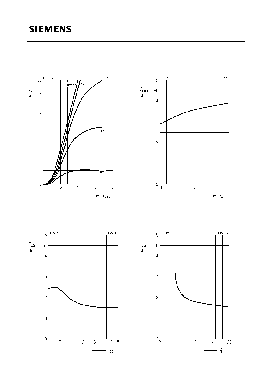
Output characteristics
I
D
=
f
(
V
DS
)
V
G2S
= 4 V
Gate 1 forward transconductance
g
fs1
=
f
(
V
G2S
)
V
DS
= 15 V,
I
DSS
= 10 mA,
f
= 1 kHz
BF 995
Semiconductor Group
5
Drain current
I
D
=
f
(
V
G1S
)
V
DS
= 15 V
Gate 2 input capacitance
C
g2ss
=
f
(
V
G2S
)
V
G1S
= 0 V,
V
DS
= 15 V
I
DSS
= 10 mA,
f
= 1 MHz
Gate 1 input capacitance
C
g1ss
=
f
(
V
G1S
)
V
G2S
= 4 V,
V
DS
= 15 V
I
DSS
= 10 mA,
f
= 1 MHz
Output capacitance
C
dss
=
f
(
V
DS
)
V
G1S
= 0 V,
V
G2S
= 4 V
I
DSS
= 10 mA,
f
= 1 MHz

BF 995
Semiconductor Group
6
Gate 1 input admittance
y
11s
V
DS
= 15 V,
V
G2S
= 4 V
(common source)
Output admittance
y
22s
V
DS
= 15 V,
V
G2S
= 4 V
(common source)
Gate 1 forward transfer admittance
y
21s
V
DS
= 15 V,
V
G2S
= 4 V
(common source)

BF 995
Semiconductor Group
7
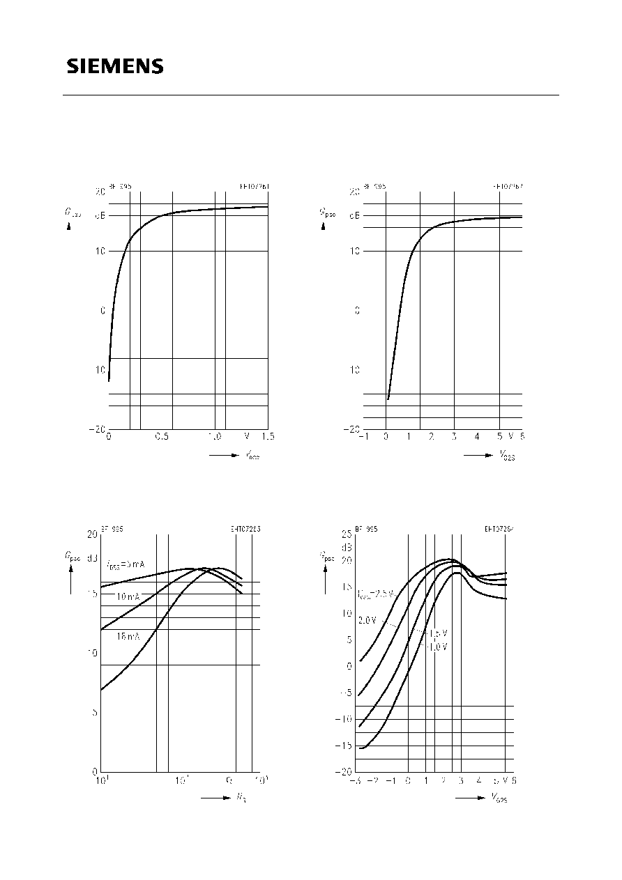
Power gain
G
ps
=
f
(
V
G2S
)
V
DS
= 15 V,
V
G1S
= 0 V,
I
DSS
= 10 mA
f
= 200 MHz (see test circuit 1)
Interference voltage for 1% cross
modulation
V
int (1%)
=
f
(
G
ps
)
1)
V
DS
= 15 V,
V
G1S
= 0,
f
= 200 MHz
f
int
= 221 MHz (see test circuit 1)
Noise figure
F
=
f
(
V
G2S
)
V
DS
= 15 V,
V
G1S
= 0 V,
I
DSS
= 10 mA
f
= 200 MHz (see test circuit 1)
Interference voltage for 1% cross
modulation
V
int (1%)
=
f
(
f
int
)
1)
V
DS
= 15 V,
V
G2S
= 4 V,
V
G1S
= 0
f
= 200 MHz (see test circuit 1)
1)
For footnote refer to the last page of this data sheet.
BF 995
Semiconductor Group
8
Mixer gain (additive)
G
psc
=
f
(
V
osc
)
V
D
= 15 V,
V
G1S
= 0,
V
G2S
= 6 V
R
S
= 220
,
I
DSS
= 10 mA,
f
= 200 MHz
f
IF
= 36 MHz (see test circuit 2)
Mixer gain (additive)
G
psc
=
f
(
R
S
)
V
D
= 15 V,
V
G1S
= 0,
V
G2S
= 6 V
V
osc
= 0.5 V,
f
= 200 MHz
f
IF
= 36 MHz (see test circuit 2)
Mixer gain (additive)
G
psc
=
f
(
V
G2S
)
V
D
= 15 V,
V
G1S
= 0,
R
S
= 220
V
osc
= 0.5 V,
I
DSS
= 10 mA,
f
= 200 MHz
f
IF
= 36 MHz (see test circuit 2)
Mixer gain (multiplicative)
G
psc
=
f
(
V
G2S
)
V
D
= 15 V,
V
G1S
= 1.7 V,
R
S
= 200
I
DSS
= 10 mA,
f
= 200 MHz
f
IF
= 36 MHz (see test circuit 3)
BF 995
Semiconductor Group
9
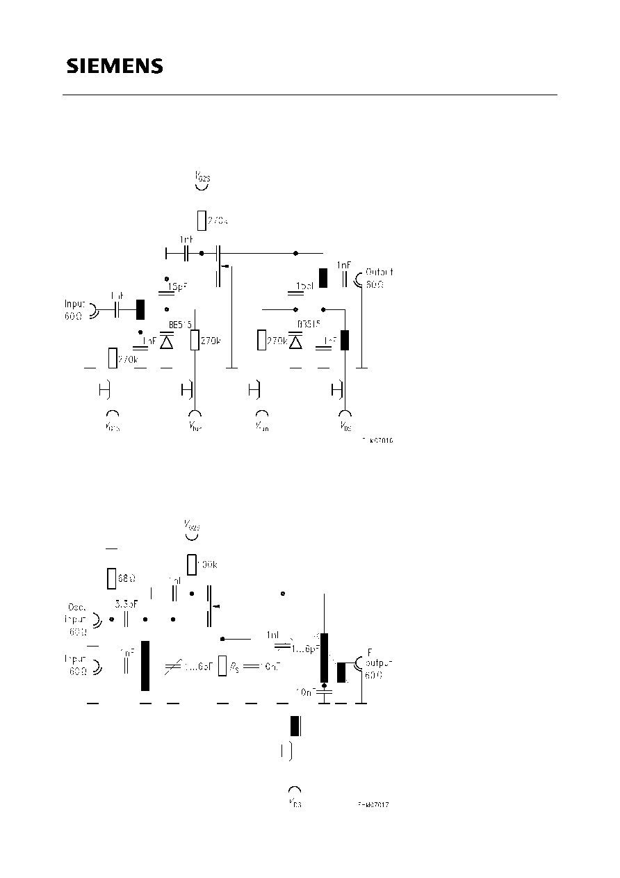
Test circuit 1 for power gain, noise figure and cross modulation
f
= 200 MHz,
G
G
= 2 mS,
G
L
= 0.5 mS
Test circuit 2 for mixer gain (additive)
f
= 200 MHz,
f
osc
= 236 MHz, 2
f
I
F
= 5 MHz

BF 995
Semiconductor Group
10
Test circuit 3 for mixer gain (multiplicative)
f
= 200 MHz,
f
osc
= 236 MHz, 2
f
IF
= 5 MHz
1)
V
int (1%)
is the rms value of half the emf (terminal voltage at matching) of a 100 % sine modulated TV carrier at
an internal generator resistance of 60
, causing 1 % amplitude modulation on the active carrier.