
Semiconductor Group
1
Aug-02-1996
BFS 17P
NPN Silicon RF Transistor
∑ For broadband amplifiers up to 1GHz at collector
currents from 1mA to 20mA
∑ CECC-type available: CECC 50002/248.
Type
Marking Ordering Code
Pin Configuration
Package
BFS 17P
MCs
Q62702-F940
1 = B
2 = E
3 = C
SOT-23
Maximum Ratings of any single Transistor
Parameter
Symbol
Values
Unit
Collector-emitter voltage
V
CEO
15
V
Collector-base voltage
V
CBO
25
Emitter-base voltage
V
EBO
2.5
Collector current
I
C
25
mA
Peak collector current
f
10 MHz
I
CM
50
Total power dissipation
T
S
55 ∞C
P
tot
280
mW
Junction temperature
T
j
150
∞C
Ambient temperature
T
A
- 65 + 150
Storage temperature
T
stg
- 65 ... + 150
Thermal Resistance
Junction - soldering point
1)
R
thJS
340
K/W
1) Package mounted on aluminia 15 mm x 16,7 mm x 0,7 mm

Semiconductor Group
2
Aug-02-1996
BFS 17P
Electrical Characteristics at
T
A
= 25∞C, unless otherwise specified.
Parameter
Symbol
Values
Unit
min.
typ.
max.
DC Characteristics of any single Transistor
Collector-emitter breakdown voltage
I
C
= 1 mA,
I
B
= 0
V
(BR)CEO
15
-
-
V
Collector-base cutoff current
V
CB
= 10 V,
I
E
= 0
V
CB
= 25 V,
I
E
= 0
I
CBO
-
-
-
-
10
0.05
µA
Emitter-base cutoff current
V
EB
= 2.5 V,
I
C
= 0
I
EBO
-
-
100
DC current gain
I
C
= 2 mA,
V
CE
= 1 V
I
C
= 25 mA,
V
CE
= 1 V
h
FE
20
20
70
-
-
150
-
Collector-emitter saturation voltage
I
C
= 10 mA,
I
B
= 1 mA
V
CEsat
-
0.1
0.4
V

Semiconductor Group
3
Aug-02-1996
BFS 17P
Electrical Characteristics at
T
A
= 25∞C, unless otherwise specified.
Parameter
Symbol
Values
Unit
min.
typ.
max.
AC Characteristics of any single Transistor
Transition frequency
I
C
= 2 mA,
V
CE
= 5 V,
f = 200 MHz
I
C
= 25 mA,
V
CE
= 5 V,
f = 200 MHz
f
T
1.3
1
2.5
1.4
-
-
GHz
Collector-base capacitance
V
CB
= 5 V,
V
BE
=
v
be
= 0 ,
f = 1 MHz
C
cb
-
0.55
0.8
pF
Collector-emitter capacitance
V
CE
= 5 V,
V
BE
=
v
be
= 0 ,
f = 1 MHz
C
ce
-
0.25
-
Input capacitance
V
EB
= 0.5 V,
I
C
= 0 ,
f = 1 MHz
C
ibo
-
1.45
-
Output capacitance
V
CE
= 5 V,
V
BE
=
v
be
= 0 ,
f = 1 MHz
C
obs
-
-
1.5
Noise figure
I
C
= 2 mA,
V
CE
= 5 V,
f = 800 MHz
Z
S
= 0
F
-
3.5
5
dB
Transducer gain
I
C
= 20 mA,
V
CE
= 5 V,
f = 500 MHz
Z
S
=
Z
L
= 50
|
S
21e
|
2
-
12.7
-
Linear output voltage
I
C
= 14 mA,
V
CE
= 5 V,
d
im
= 60 dB
f
1
= 806 MHz,
f
2
= 810 MHz,
Z
S
=
Z
L
= 50
V
01
=
V
02
-
100
-
mV
Third order intercept point
I
C
= 14 mA,
V
CE
= 5 V,
f = 800 MHz
Z
S
=
Z
Sopt,
Z
L
=
Z
Lopt
IP
3
-
23
-
dBm
Semiconductor Group
4
Aug-02-1996
BFS 17P
Total power dissipation
P
tot
=
f (T
A
*,
T
S
)
* Package mounted on epoxy
0
20
40
60
80
100
120 ∞C 150
T
A
,T
S
0
50
100
150
200
mW
300
P
tot
T
S
T
A
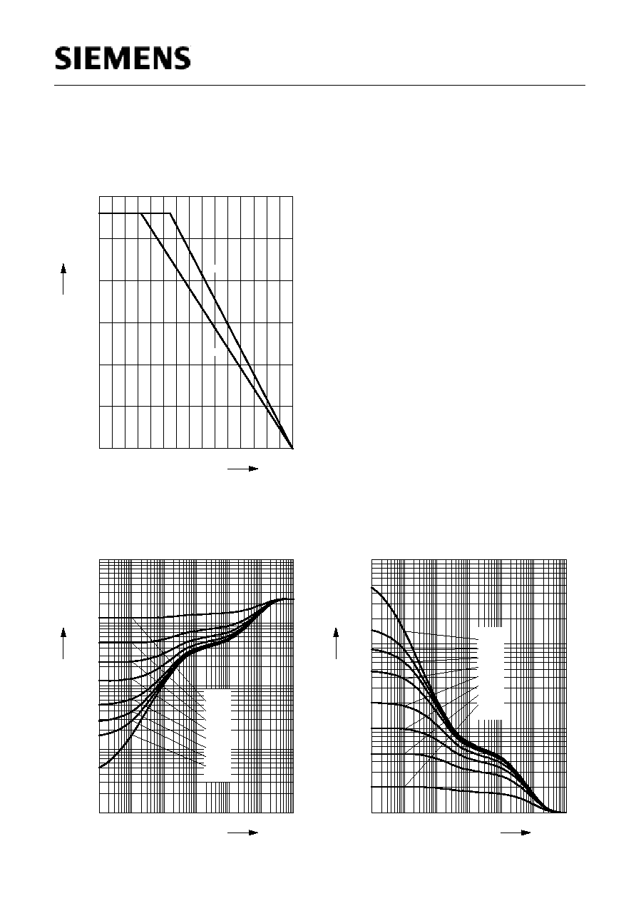
Permissible Pulse Load
R
thJS
=
f (t
p
)
10
-6
10
-5
10
-4
10
-3
10
-2
10
-1
10
0
s
t
p
-1
10
0
10
1
10
2
10
3
10
K/W
R
thJS
D = 0
0.005
0.01
0.02
0.05
0.1
0.2
0.5
Permissible Pulse Load
P
totmax
/
P
totDC
=
f (t
p
)
10
-6
10
-5
10
-4
10
-3
10
-2
10
-1
10
0
s
t
p
0
10
1
10
2
10
3
10
-
P
totmax
/
P
totDC
D = 0
0.005
0.01
0.02
0.05
0.1
0.2
0.5
Semiconductor Group
5
Aug-02-1996
BFS 17P
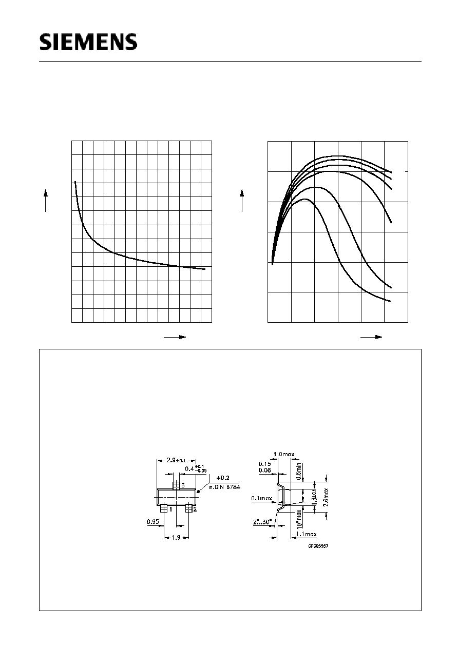
Collector-base capacitance
C
cb
=
f (V
CB
)
V
BE
=
v
be
= 0,
f = 1MHz
0
4
8
12
16
20
V
26
V
CB
0.0
0.1
0.2
0.3
0.4
0.5
0.6
0.7
0.8
0.9
1.0
1.1
pF
1.3
C
cb
Transition frequency
f
T
=
f (I
C
)
f = 500MHz
V
CE
= Parameter
0
5
10
15
20
mA
30
I
C
0.0
0.5
1.0
1.5
2.0
GHz
3.0
f
T
10V
5V
3V
2V
1V
0.7V
Package