Semiconductor Group
1
PNP Silicon RF Transistor
BF 550
q
For common emitter amplifier stages
up to 300 MHz
q
For mixer applications in AM/FM radios
and VHF TV tuners
q
Low feedback capacitance
due to shield diffusion
q
Controlled low output conductance
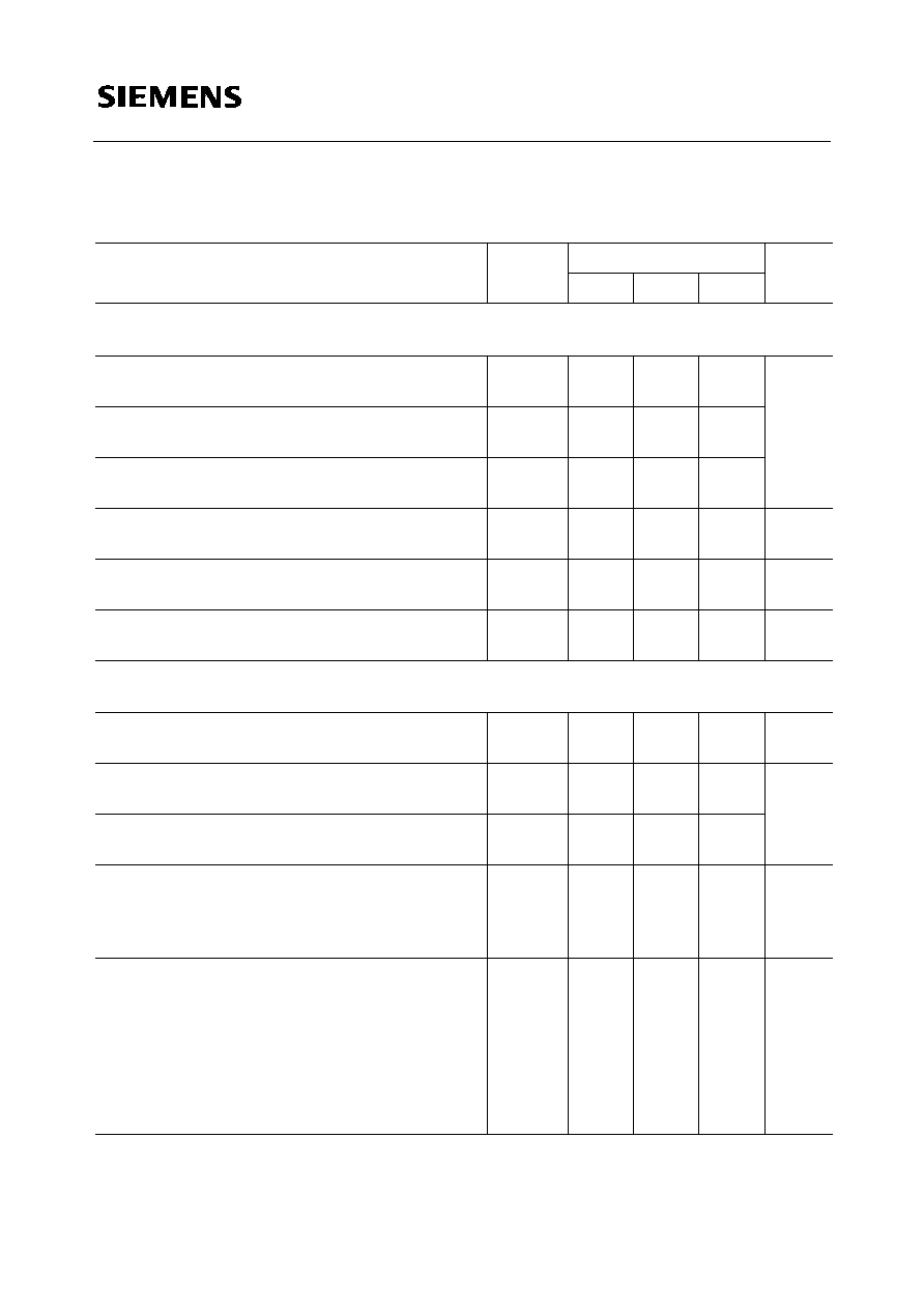
Maximum Ratings
Type
Ordering Code
(tape and reel)
Marking
Package
1)
Pin Configuration
BF 550
Q62702-F944
LA
SOT-23
1
2
3
B
E
C
Parameter
Symbol
Values
Unit
Collector-emitter voltage
V
CE0
40
V
Collector-base voltage
V
CB0
40
Emitter-base voltage
V
EB0
4
Thermal Resistance
Junction - ambient
2)
R
th JA
450
K/W
Total power dissipation,
T
A
25 �C
P
tot
280
mW
Storage temperature range
T
stg
� 65 ... + 150
Base current
I
B
5
Junction temperature
T
j
150
�C
Collector current
I
C
25
mA
1)
For detailed information see chapter Package Outlines.
2)
Package mounted on alumina 15 mm
�
16.7 mm
�
0.7 mm.
07.94
BF 550
Semiconductor Group
2
Electrical Characteristics
at
T
A
= 25 �C, unless otherwise specified.
Unit
Values
Parameter
Symbol
min.
typ.
max.
DC Characteristics
AC Characteristics
V
Collector-emitter breakdown voltage
I
C
= 1 mA,
I
B
= 0
V
(BR) CE0
40
�
�
Collector-base breakdown voltage
I
C
= 10
�
A,
I
E
= 0
V
(BR) CB0
40
�
�
Emitter-base breakdown voltage
I
E
= 10
�
A,
I
C
= 0
V
(BR) EB0
4
�
�
nA
Collector cutoff current
V
CB
= 30 V,
I
E
= 0
I
CB0
�
�
100
�
DC current gain
I
C
= 1 mA,
V
CE
= 10 V
h
FE
50
�
250
V
Base-emitter voltage
I
C
= 1 mA,
V
CE
= 10 V
V
BE
�
0.72
�
MHz
Transition frequency
I
C
= 1 mA,
V
CE
= 10 V,
f
= 100 MHz
f
T
�
350
�
pF
Collector-base capacitance
V
CB
= 10 V,
V
BE
= 0 V,
f
= 1 MHz
C
cb
�
0.33
�
Collector-emitter capacitance
V
CE
= 10 V,
V
BE
= 0 V,
f
= 1 MHz
C
ce
�
0.67
�
dB
Noise figure
V
CE
= 10 V
I
C
= 1 mA,
f
= 100 kHz,
R
S
= 300
I
C
= 2 mA,
f
= 100 MHz,
R
S
= 60
F
�
�
2
3.4
�
�
�
S
pF
mS
pF
�
S
�
S
f
= 0.45 ... 10 MHz
f
= 500 kHz
f
= 10 MHz
g
11e
C
11e
I
y
21e
I
C
22e
g
22e
g
22e
�
�
�
�
�
�
550
17
35
1.3
5
5
�
�
�
�
8
10
Y parameters, common emitter
I
C
= 1 mA,
V
CE
= 10 V