
BGA 310
Semiconductor Group
Sep-04-1998
1
Silicon Bipolar MMIC-Amplifier
Preliminary data
∑
Cascadable 50
-gain block
∑
9 dB typical gain at 1.0 GHz
∑
9 dBm typical
P
-1dB
at 1.0 GHz
∑
3 dB-bandwidth: DC to 2.4 GHz
VPS05178
2
1
3
4
EHA07312
3
1
2, 4
RF IN
RF OUT/Bias
GND
Circuit Diagram
Type
Marking Ordering Code
Pin Configuration
Package
BGA 310 BLs
Q62702-G0041
1 RFout/bias 2 GND 3 RF input
4 GND SOT-143
Maximum Ratings
Parameter
Value
Symbol
Unit
Device current
I
D
mA
60
Total power dissipation,
T
S
99 ∞C
250
P
tot
mW
R
F
input power
dBm
10
P
RFin
T
j
Junction temperature
150
∞C
Ambient temperature
T
A
-65 ...+150
Storage temperature
T
stg
-65 ...+150
Thermal Resistance
Junction - soldering point
1)
R
thJS
205
K/W
1)
T
S
is measured on the collector lead at the soldering point to the pcb
Semiconductor Group
1
1998-11-01

BGA 310
Semiconductor Group
Sep-04-1998
2
Electrical Characteristics at
T
A
= 25 ∞C, unless otherwise specified.
Parameter
Values
Symbol
Unit
max.
typ.
min.
AC characteristics (
V
D
= 4.7 V,
Z
o
= 50
)
dB
10
9
8
-
-
-
-
-
-
|
S
21
|
2
Insertion power gain
f = 0.1 GHz
f = 1 GHz
f = 1.8 GHz
Insertion point gain flatness
f = 0.1 GHz to 0.6 GHz
-
|
S
21
|
2
-
+-0.5
Noise figure
f = 0.1 GHz
f = 1 GHz
f = 2 GHz
NF
6
6.5
7
-
-
-
-
-
-
1dB compression point
f = 1 GHz
P
-1dB
-
dBm
-
9
Return loss input
f = 0.1 GHz to 2 GHz
RL
in
-
20
-
dB
Return loss output
f = 0.1 GHz to 3 GHz
RL
out
-
15
-
Typical biasing configuration
EHA07313
D
V
RFC (optional)
IN
C
Block
Block
C
OUT
D
Bias
R
min.
CC
V = 7 V
1
3
2
4
R
Bias
=
V
CC
-
V
D
/
I
D
V
D
= 4.7V
Semiconductor Group
2
1998-11-01

BGA 310
Semiconductor Group
Sep-04-1998
3
S-Parameters at
T
A
= 25 ∞C
f
S
11
S
22
S
12
S
21
ANG
ANG
MAG
MAG
MAG
ANG
GHz
MAG
ANG
V
D
= 4.7 V,
Z
o
= 50
0.01
0.1
0.3
0.5
0.8
1
1.8
2.4
3
0.051
0.053
0.053
0.058
0.054
0.049
0.053
0.161
0.257
176.4
168.1
141.9
123.9
98.2
86.1
-164.9
-177.7
153.9
3.22
3.23
3.22
3.2
3.17
3.12
2.79
2.41
2.03
179.3
174.9
164.6
154.2
138.7
128.4
88
60.8
38.2
0.149
0.149
0.15
0.152
0.157
0.162
0.188
0.208
0.225
0.2
1.2
3.4
5.4
8.1
9.7
12
10.6
8.2
0.159
0.158
0.157
0.155
0.153
0.153
0.16
0.168
0.178
-0.5
-6.1
-19
-31.7
-51.3
-64.3
-106.6
-123.7
-133.1
Insertion power gain |
S
21
|
2
=
f ( f )
V
D
= 4.7 V,
I
D
= 42 mA
10
-1
10
0
10
1
GHz
f
0
5
10
15
dB
25
|
S
21
|
2
Noise figure
NF = f ( f )
V
D
= 4.7 V,
I
D
= 42 mA
10
-1
10
0
10
1
GHz
f
0
2
4
6
dB
10
NF
Semiconductor Group
3
1998-11-01
BGA 310
Semiconductor Group
Sep-04-1998
4
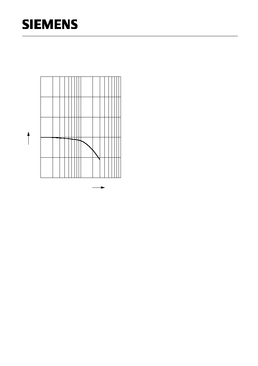
Output power 1-dB-gain compression
P
-1dB
=
f ( f )
V
D
= 4.7 V,
I
D
= 42 mA
10
-1
10
0
10
1
GHz
f
0
5
10
15
dBm
25
P
-1dB
Semiconductor Group
4
1998-11-01