
BGA 312
Semiconductor Group
Sep-04-1998
1
Silicon Bipolar MMIC-Amplifier
Preliminary data
∑
Cascadable 50
-gain block
∑
11 dB typical gain at 1.0 GHz
∑
9 dBm typical
P
-1dB
at 1.0 GHz
∑
3 dB-bandwidth: DC to 2.0 GHz
VPS05178
2
1
3
4
EHA07312
3
1
2, 4
RF IN
RF OUT/Bias
GND
Circuit Diagram
Type
Marking Ordering Code
Pin Configuration
Package
BGA 312 BMs
Q62702-G0042
1 RFout/bias 2 GND 3 RFinput
4 GND SOT-143
Maximum Ratings
Parameter
Value
Symbol
Unit
Device current
I
D
mA
60
Total power dissipation,
T
S
99 ∞C
250
P
tot
mW
R
F
input power
dBm
10
P
RFin
T
j
Junction temperature
150
∞C
Ambient temperature
T
A
-65 ...+150
Storage temperature
T
stg
-65 ...+150
Thermal Resistance
Junction - soldering point
1)
R
thJS
205
K/W
1)
T
S
is measured on the collector lead at the soldering point to the pcb
Semiconductor Group
1
1998-11-01
BGA 312
Semiconductor Group
Sep-04-1998
2
Electrical Characteristics at
T
A
= 25 ∞C, unless otherwise specified.
Parameter
Values
Symbol
Unit
max.
typ.
min.
AC characteristics (
V
D
= 4.7 V,
Z
o
= 50
)
dB
12
11
10
-
-
-
-
-
-
|
S
21
|
2
Insertion power gain
f = 0.1 GHz
f = 1 GHz
f = 1.8 GHz
Insertion point gain flatness
f = 0.1 GHz to 0.6 GHz
-
|
S
21
|
2
-
+-0.6
Noise figure
f = 0.1 GHz
f = 1 GHz
f = 2 GHz
NF
5.5
6
7
-
-
-
-
-
-
1dB compression point
f = 1 GHz
P
-1dB
-
dBm
-
9
Return loss input
f = 0.1 GHz to 2 GHz
RL
in
-
20
-
dB
Return loss output
f = 0.1 GHz to 3 GHz
RL
out
-
14
-
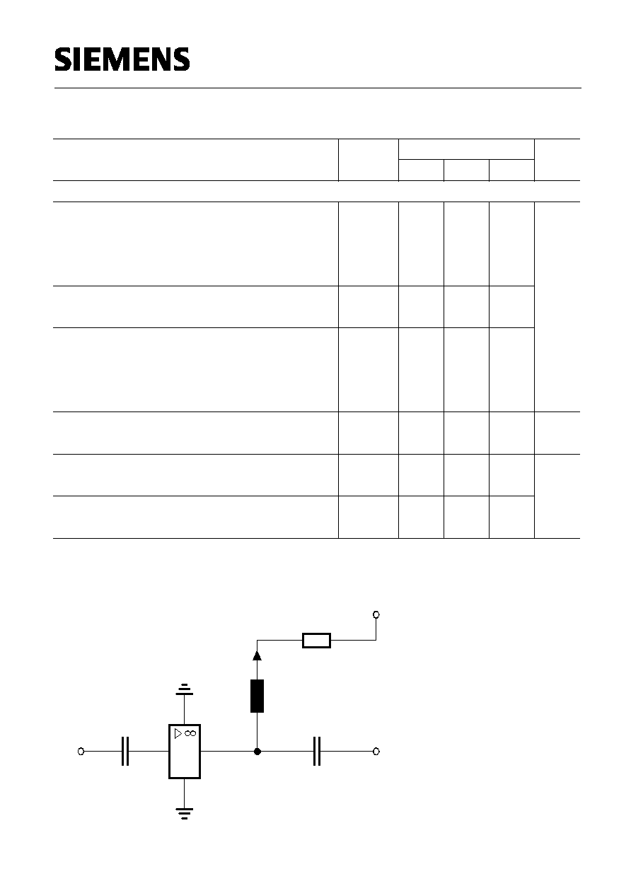
Typical biasing configuration
EHA07313
D
V
RFC (optional)
IN
C
Block
Block
C
OUT
D
Bias
R
min.
CC
V = 7 V
1
3
2
4
R
Bias
=
V
CC
-
V
D
/
I
D
V
D
= 4.7V
Semiconductor Group
2
1998-11-01

BGA 312
Semiconductor Group
Sep-04-1998
3
S-Parameters at
T
A
= 25 ∞C
f
S
11
S
22
S
12
S
21
ANG
ANG
MAG
MAG
MAG
ANG
GHz
MAG
ANG
V
D
= 4.7 V,
Z
o
= 50
0.01
0.1
0.3
0.5
0.8
1
1.8
2.4
3
0.009
0.012
0.027
0.039
0.049
0.046
0.054
0.147
0.24
17.9
43.5
55.8
52.5
33.7
22.2
-135.4
179.9
152.1
3.94
3.95
3.93
3.89
3.79
3.69
3.13
2.63
2.19
179.2
174.4
163.4
152.2
135.8
124.9
84.1
57.6
35.7
0.131
0.131
0.133
0.136
0.142
0.149
0.181
0.205
0.225
0.2
1.7
4.8
7.8
11.7
13.8
16.6
14.7
11.6
0.208
0.207
0.204
0.201
0.194
0.191
0.183
0.182
0.184
-0.5
-6.2
-19.1
-31.9
-51.3
-64.2
-106.8
-124.9
-134.9
Insertion power gain |
S
21
|
2
=
f ( f )
V
D
= 4.7 V,
I
D
= 42 mA
10
-1
10
0
10
1
GHz
f
0
5
10
15
dB
25
|
S
21
|
2
Noise figure
NF = f ( f )
V
D
= 4.7 V,
I
D
= 42 mA
10
-1
10
0
10
1
GHz
f
0
2
4
6
dB
10
NF
Semiconductor Group
3
1998-11-01
